We are honored to welcome distinguished experts and professors from Taiwan and Europe as speakers for this forum. They bring extensive experience and strong academic backgrounds in semiconductor research, IC design, advanced packaging, and silicon photonics, and have made significant contributions to industry-academia collaboration and innovative applications. During the forum, they will share insights on emerging technologies, research breakthroughs, and practical industry trends, offering participants valuable learning opportunities and professional inspiration.
European Semiconductor Manufacturing Company (ESMC)
Christian Koitzsch
Dr. Christian Koitzsch has been the president and managing director of the European Semiconductor Manufacturing Company (ESMC) since beginning of 2024. He was raised in Thueringia, is married and is father of two children. He studied electrical engineering at Technische Universität Ilmenau and North Carolina State University in Raleigh (US) and received a PhD in solid state physics from the University of Neuchâtel, Switzerland.
Professional milestones
2004 ABB Semiconductors, Process engineer, Lenzburg (CH)
2007 Ersol Solar Energy AG, Manager silicon material procurement, Thüringen
2008 Bosch Solar Thin Film, Managing Director, Thüringen
2012 Robert Bosch GmbH, Office of the chairman of the supervisory board, Baden-Württemberg
2015 Robert Bosch India (RBEI), Vice President and Key account manager Automotive Electronics, Bengaluru (Indien)
2018 Robert Bosch GmbH, Senior Vice President Corporate Advance Engineering and Research, Baden-Württemberg
2021 Robert Bosch Semiconductor Manufacturing GmbH, Plant Manager and Managing Director, Dresden
2024 President and Managing Director ESMC
TOPIC: ESMC – a light house project of the European chips actin Silicon Saxony
ESMC, a joint venture between Bosch, Infineon, NXP and TSMC, is establishing an advanced logic foundry operation in Dresden, Germany. The facility will be a first-of-its-kind 12 nm FINFET open EU foundry. The talk will present the current status and future plans of the project. Special emphasis is given to sustainability and development of the local talent and ecosystem.
Synopsys/R&D
Sander Roosendaal
Sander Roosendaal is a senior R&D leader at Synopsys, where he drives the development of the Photonic Integrated Circuit design suite.
With a Ph.D. in Physics from Utrecht University, Sander began his career as a scientist at Philips Research, contributing to and leading industrial R&D in the fields of Liquid Crystal Displays and electronic paper.
From 2008 to 2020, Sander served as a program manager and technical leader at Honeywell Aerospace, overseeing Honeywell’s involvement in the Single European Sky ATM Research (SESAR) joint undertaking.
In this role, he managed EU-funded projects and consortia and led a team of 50+R&D engineers, honing his expertise in large-scale program management and cross-disciplinary collaboration.
Since 2020, Sander has been the R&D leader for Photonic Systems at Synopsys, where he bridges the gap between physics (photonics) and professional software development. His interests span program management, industrial R&D,innovation, numerical simulation, and software development, with a particularpassion for projects where these fields intersect to create cutting-edgetechnologies.
TOPIC: The Power of PhotonicICs in Next Gen Datacenters
As artificial intelligence workloads scale exponentially, modern datacenters face unprecedented demands for bandwidth and energy efficiency. Traditional electrical interconnects are increasingly inadequate, with I/O power consumption now dominating overall system energy budgets. This presentation explores how Photonic Integrated Circuits (PICs),particularly in co-packaged optics (CPO) configurations, are transforming datacenter architectures to meet these challenges. We examine the key challenges in optical transceiver design—from device-level innovations to architectural and packaging complexities—and show how a robust design flow can enable first-time-right implementation of these advanced systems.
CARL ZEISS CO. Ltd
Charles Lin
Mr. Charles Lin had over 25 years’ experience for semiconductor and microscopy characterization, Since joining Carl Zeiss as a Sr. Application & Business Development Manager in2023, currently is manage for ZEISS Innovation Center in Hsinchu(TW), lead the application team and host RD development cooperation project with key partner, previously work in FEI/TMO for more than 16 years and AMAT & Bruker for rest, most experienced in SEM/FIB/TEM technology for Failure analysis, yield enhancement and metrology, also implement in-line wafer-level TEM workflow solution for RD development, experienced on E-beam inspection & review, X-ray inspection& metrology for front-end, back-end & advance package, participated the new technology launch to meet RD & production demand.
TOPIC: The impact of 3DX-ray Microscope in Next Gen AI Chips
As advanced packaging architectures evolve with increasing density and feature scaling ,larger footprints are required to accommodate more components, supporting the heterogeneous integration and More-than-Moore innovations. These trends bring new challenges in inspection, failure analysis and materials characterization, necessitating advancements in analytical tools, techniques, and workflows.
This presentation discusses recent progress in two key techniques gaining prominence in advanced packaging: 3D X-ray microscopy (XRM) and laser-integrated focused ion beam scanning electron microscopy (LaserFIB). The integration of fs-laser technology enhances cross-section preparation throughput and enables site-specific analysis of buried features. Using minimal damage, a thermal material removal capabilities of the fs laser, combined with correlative technique from 3D XRM imaging, allows for precise targeting and high-throughput analysis of complex structures, including high resolution SEM imaging, EDS and EBSD.
The 3D XRM to LaserFIB correlative workflow marks a significant advancement in addressing the challenges of failure analysis in next-generation advanced packaging.
Taiwan Semiconductor Manufacturing Company(TSMC)
Glavine Yeh
Glavine Yeh is a Senior Program Manager at TSMC Europe. He joined TSMC in 1997 and he began as a process engineer and then taking the role of Manager of Customer Service for the Japan region. In 2008, Glavine transitioned to TSMC Europe as a Technical Manager, where he focused on driving technology engagement and enabling new product development. He played a pivotal role in advancing embedded non-Volatile Memory (eNVM) technologies, successfully positioning eNVM as one of the fastest-growing business areas for TSMC Europe. Following his technical role, Glavine took charge of the university FinFET program, fostering innovation within EMEA academia through advanced technologies. Additionally, he oversaw marketing events across the EMEA region, further strengthening TSMC’s presence in the area.
TOPIC: Collaborations on Semiconductor Research& Talent Incubation
Semiconductors have been instrumental in transforming human life, driving rapid advancements across numerous domains. The proliferation of personal computers, the internet, mobile devices, and high-performance computing (HPC) servers has introduced immense computing power and connectivity into everyday lives.
As we progress into the era of Artificial Intelligence (AI), advanced semiconductor technologies are emerging as essential enablers, providing the computational power, memory capacity, and data transfer bandwidth required for AI applications.
TSMC is the important enabler for the ear of artificial intelligence. Academia is the foundation of the future talents for the semiconductor industry. In this presentation, The talk will present TSMC overall talent incubation programs, including different collaboration model, FinFET program and the development of latest status.

SiCADA
Yung Wuu
Dr. Tzyh-Yung Wuu (AKA Yung Wuu) currently serves as the President of SiCADA (Silicon Creation and Advance Design Academy). He has previously held positions as Vice President of Engineering and Senior Director at Synopsys US for over 20 years, as well as Product Development Manager at AVANT! CORP.
With over 30 years of experience in the semiconductor design software industry, Dr. Wuu has navigated through both startup ventures and large corporations, gaining extensive expertise in technical research and development, customer support, and on-the-job training. His proficiency spans product strategy, market development, and technological innovation, excelling in leading teams to establish comprehensive solutions, supporting customers in successful product development, and driving business growth.
Yung Wuu holds a Ph.D. in Computer Engineering from the University of Southern California and a bachelor’s degree in electronic engineering from National Chiao Tung University.
TOPIC: IC Talent Cultivation in the AI Era
Academia provides students with foundational knowledge and fosters creativity, while industry enables them to create high-value products. Rapid advancements in semiconductor technology have widened the gap between academic preparation and the practical skills demanded by the field. In the AI era, engineers could further enhance productivity by leveraging AI-powered tools. Experienced IC engineers play a crucial role in bridging this gap by mentoring the next generation, helping them integrate theoretical knowledge with industry-relevant skills, best practices, and the latest AI-driven solutions. This presentation shares our experience in integrating resources from industry, government, academia, and research, as well as the use of artificial intelligence, to help close the gap between learning and industry needs.
Interuniversity Microelectronics Centre (imec), Belgium & Europractice
Romano Hoofman
Romano Hoofman is Strategic Development Director at imec since 2016. He is currently responsible for the innovation programs at IC-Link and for the coordination of both the EU Chips Design Platform and the EUROPRACTICE Service.
He started his career in industry, where he worked as a Principal Scientist at Philips Research and later on NXP Semiconductors. He covered many different R&D topics, ranging from CMOS integration, advanced packaging, thin film batteries, photovoltaics and (bio)sensors.
Romano received his PhD from the Technical University of Delft in 2000, where he investigated charge transport in semi-conducting polymers. He has authored more than 30 publications and holds more than 10 patents in various research areas.
Title: Europractice and Beyond: Empowering Europe's Semiconductor Innovation under the Chips Act.
For more than 30 years, imec has lowered the barrier to access design tools and fabrication technologies for universities, research centres and their spinouts such that they can innovate with novel integrated circuit solutions.
One of the fundaments of these activities is Europractice. Since 1989, Europractice has functioned as a one-stop-shop that supports all critical steps from prototype design to volume production.
Recently, under the EU Chips Act more actions have been launched to boost semiconductor innovation in Europe.
The Chips for Europe Initiative is the first pillar of the European Chips Act, a comprehensive strategy to strengthen the EU's semiconductor ecosystem. It aims to support large-scale technology capacity-building and foster innovation.
In this talk, I will highlight imec’s role in the first pillar of the EU Chips Act, in particular, the NanoIC pilot line and the EU Chips Design Platform, and how these initiatives can grow Europe’s design and technological leadership.
National Center for High-Performance Computing, National Institute of Applied Research (NCHC, NIAR)
An-Cheng Yang
Driven by a passion for innovation atthe National Center for High-performance Computing, I leveraged HighPerformance Computing and collaborative skills to enhance research capabilities.My expertise in Machine Learning and mentorship at National Yang Ming ChiaoTung University underscore my commitment to advancing Material Informatics. I recentlybegan advancing quantum computing applications in scientific computing.
· https://scholar.google.com/citations?user=Bf_9y0AAAAAJ&hl=zh-TW
2012-12 - Current
Associate Researcher
National Center For High-performance Computing, Hsinchu
· Collaborated closely with interdisciplinary teams.
2019-02 - 2023-07
Adjunct Associate Professor
National Yang Ming Chiao Tung University, Hsinchu
· Machine Learning on Material Informatics.
Education
2011-06
Ph.D.: Mechanical Engineering
National Cheng Kung University - Tainan City, Taiwan
2004-06
M.E.: Mechanical Engineering
National Cheng Kung University - Tainan City, Taiwan
2002-06
B.E.: Mechanical Engineering
National Chiao Tung University - Hsinchu, Taiwan
TOPIC: Partnership of NCHC and TSRI on Semiconductor fabrication
This talk presents the collaborative achievements between the National Center for High-Performance Computing (NCHC) and the Taiwan Semiconductor Research Institute (TSRI) in advancing semiconductor fabrication technologies. We first introduce the co-developed secure cloud architecture, which enables protected access, data confidentiality, and compliant workflows for semiconductor R&D and cross-institution collaboration. Building on this foundation, we highlight the development of AI-assisted device design workflows, including model training, parameter optimization, and distributed simulation, which collectively accelerate component development and innovation. Finally, we discuss the application of digital twin technology in semiconductor talent cultivation. By providing an integrated virtual–physical process simulation environment, digital twins allow students, researchers, and industrial trainees to practice skills in a safe, reproducible, and scalable setting, strengthening the talent development ecosystem for the semiconductor industry.
National Center for Instrumentation Research, National Institute of Applied Research (NCIR, NIAR)
Wei-Lin Wang
Wei-Lin Wang is currently an Associate Researcher at National Center for Instrumentation Research (NCIR), National Institute of Applied Research (NIAR). He received his Ph.D. in Materials Science and Engineering from National Chiao Tung University (NCTU) in 2011, now known as National Yang Ming Chiao Tung University (NYCU). From 2011 to 2013, he worked at Ubilux Optoelectronics Corporation on nitride epitaxial growth for blue light–emitting diodes (LEDs). He later joined Powerchip Semiconductor Manufacturing Corporation (2013–2023), where he was responsible for thin-film processing, process integration, tape-out, process design and product development. He joined NCIR in 2023, focusing on system development and metalorganic chemical vapor deposition (MOCVD) processes.
TOPIC: Advanced Semiconductor Thin-Film Technologies with MOCVD
Dr. Wang will highlight National Center for Instrumentation Research(NCIR) of National Institutes of Applied Research (NIAR) and its role in advancing semiconductor materials and processes. As the semiconductor industry continues to rapidly evolve, the development of next-generation materials and deposition technologies has become essential. In this talk, Dr. Wang will present NCIR’s current efforts in metalorganic chemical vapor deposition(MOCVD), focusing on two major research directions: two-dimensional transition metal dichalcogenides (2D TMDCs) and wide–band gap metal oxides such as gallium oxide (Ga₂O₃). 2D TMDCs are promising materials for high-performance electronics, while Ga₂O₃ offers exceptional potential in high-power and high-voltage devices due to its ultra-wide band gap. Over the past several years, NCIR has built its own MOCVD systems, developed thin-film processes, and established a mature platform capable of producing wafers. These achievements enable NCIR to actively collaborate with both academic institutions and industrial partners, driving innovation in material growth, process optimization, and device-oriented research.
Taiwan Semiconductor Research Institute, National Institute of Applied Research (TSRI, NIAR)
Hsin-Hao Liao
Hsin-Hao Liao is an Associate Engineer at the Heterogeneous Chip Integration Division of the Taiwan Semiconductor Research Institute(TSRI), part of the National Institute of Applied Research (NIAR). He received the M.S. degree in Chemical Engineering from National Tsing Hua University, Hsinchu, Taiwan, in 1998. From 2000 to 2009, he worked as a Process Integration and Etch Process Principal Engineer at Taiwan Semiconductor Manufacturing Company (TSMC), Hsinchu, Taiwan. In 2009, he joined TSRI, where he focused on the development and academic promotion of CMOS-MEMS and BioMEMS platforms. His current research and engineering activities involve 2.5D and 3D heterogeneous integration processes and technologies, as well as serving as a technical service contact for domestic and international customers.
TSRI 2.5D-3D Heterogeneous Integration Platform and Demonstration Showcase
The Taiwan Semiconductor Research Institute (TSRI) has developed a 2.5D–3D heterogeneous integration (HI) platform to support advanced multi-chip module research across academia and startups. The platform integrates chip-on-chip-on-PCB(CoCoB) stacking, active silicon interposers with through-silicon vias(TSVs), and micro-bump technology (50 µm pitch), providing a low-cost, scalable path for prototyping AIoT, HPC, and sensor systems. Using TSMC 0.18 µm AlCu CMOS process, TSRI achieves active CMOS interposers with low resistance (< 2 Ω) and high isolation (> 3 MΩ), supported by in-house gold-stub bumping capability. Primary heterogeneous integration demonstrations—including ASIC-to-ASIC,ASIC-sensor, and biosensor hybrids —validate both electrical and mechanical feasibility across diverse technology nodes and device types, and further integrated voltage regulators (IVR) will be involved in near future. This platform establishes a unified academic framework for heterogeneous chip integration, fostering cross-domain innovation in advanced packaging and system-on-interposer design.
Taiwan Semiconductor Research Institute, National Institute of Applied Research (TSRI, NIAR)
Ming-Wei Lin
Ming-Wei Lin is an Associate Researcher at the Heterogeneous Chip Integration Division of the Taiwan Semiconductor Research Institute (TSRI), part of the National Institute of Applied Research (NIAR). He received his Ph.D. in Photonics from National Cheng Kung University in 2013 and joined TSRI in 2017 to advance silicon photonics and co-packaged optics (CPO) technologies. His expertise spans high-speed modulator and photodetector design, physical layout implementation, and tape-out coordination with commercial foundries such as imec and TSMC. Dr. Lin has led the design and characterization of multiple electronic–photonic integrated circuits (EPICs) and developed high-frequency optoelectronic test platforms supporting 200G/400G PAM4 measurements up to 110 GHz. His research integrates photonic circuit design, heterogeneous material integration, and advanced 3D packaging strategies, enabling wafer- and package-level validation toward next-generation CPO systems.
TOPIC: Advancing Silicon Photonics and Co-Packaged Optics Integration
The rapid evolution of data center and high-performance computing applications demands scalable and energy-efficient optical interconnects. This talk presents the recent progress of the Taiwan Semiconductor Research Institute (TSRI) in developing a comprehensive silicon photonics platform that bridges photonic–electronic design, heterogeneous material integration, and high-speed packaging technologies. The presentation will also highlight the collaborative efforts between TSRI and European partners such as imec. Together, these efforts aim to accelerate the realization of a robust SiPh–CPO ecosystem for next-generation optical computing and communication systems.

Taiwan Semiconductor Research Institute, National Institute of Applied Research (TSRI, NIAR)
Sheng-Hsiang Tseng
Sheng-Hsiang Tseng received his Ph.D. from the Institute of Electronics Engineering at National Tsing Hua University, Hsinchu, Taiwan. He joined the National Chip Implementation Center, Hsinchu, Taiwan, in 2002. He is currently a Research Fellow and also serves as the Director of the Chip Implementation Service Division at the Taiwan Semiconductor Research Institute (TSRI), Hsinchu, Taiwan. His research interests include CMOS-based MEMS ICs, MEMS technologies, piezoelectric MEMS, RF MEMS, heterogeneous chip integration, and packaging technologies. He has been recognized with multiple awards for outstanding contributions to science and technology from the National Institutes of Applied Research (NIAR). Dr. Tseng was the recipient of the Young Engineer Award from the Taiwan Nanotechnology and Micro System Association (NMA) in 2022. He served on the Technical Committee on Sensors, MEMs, and Bioelectronics (SMB) of IEEE IEDM from 2021 to 2022. He currently also serves as the Secretary-General of the NMA in Taiwan.
TOPIC: TSRI MEMS Design & Verification Platform: Powering the Smart Sensing SIG
In this talk, Dr. Tseng will present the design environment and implementation services of the CMOS-MEMS and MEMS Chip Design and Verification Platform developed by TSRI. He will also outline the mission and key initiatives of the Smart Sensing Special Interest Group (SIG), which was officially launched in 2025. The SIG is dedicated to fostering international academic and research collaboration in design verification and chip fabrication, with the broader goal of enhancing global engagement and strengthening research partnerships between Taiwan and the international community.
Interuniversity Microelectronics Centre (imec), Belgium
Yasser Sherazi
S. M. Yasser Sherazi received his B.Sc. degree in Computer Engineering from the COMSATS Institute of Information Technology, Islamabad, Pakistan, in 2005, and his M.Sc. degree in System-on-Chip Design from Linköping University, Sweden, in 2008. He earned his Ph.D. in Digital ASIC Design in 2014 from the Department of Electrical and Information Technology at Lund University, Sweden, where his research focused on design space exploration and the development of ultra-low-energy digital circuits for wireless baseband applications.
He joined imec, Belgium, as a postdoctoral researcher, working on digital gate and design technology co-optimization for 10nm technologies. In 2016, he became an R&D Specialist at imec, leading efforts in standard cell architecture development for advanced technology nodes such as 5nm and 3nm. From 2018 to 2024, he managed the design team responsible for 300mm wafer-based test vehicle development.
Dr. Sherazi currently serves as Group Manager of the RIDE (Research Infrastructure for Design Enablement) group at imec, which focuses on developing R&D Process Design Kits (PDKs) for advanced scaling nodes.
TOPIC: imec’s Technology Roadmap with Respect to Lithography, Logic, and Memory, Leading to the Era of CMOS 2.0
Scaling silicon technology has become increasingly challenging, demanding a holistic approach to sustain the progress traditionally captured by Moore’s Law. Advancing to next-generation technology nodes requires optimization across multiple dimensions—lithography, device architecture, memory integration, and system-level design.
In this presentation, we will review imec’s lithography roadmap, spanning nodes from N3/N2 through A14,A10, A7, A5, and A3/A2, and discuss how it aligns with logic device innovations and standard cell evolution. We will also explore emerging memory options and their role in achieving balanced performance, power, and density targets. Finally, we will highlight the importance of cross-technology co-optimization as the foundation for CMOS 2.0, the next paradigm in semiconductor scaling.

Fraunhofer IPMS, Center Nanoelectronic Technologies, Germany
Thomas Kämpfe
Thomas Kämpfe serves as a Full Professor at TU Braunschweig as well as Head of Department Components & Systems as well as Group Manager for Neuromorphic Systems at Fraunhofer IPMS. He earned his habilitation in electrical engineering in 2022and his Ph.D. in Physics in 2016, both from TU Dresden. Following research scholar positions at the University of Colorado at Boulder and Stanford University, he joined the Fraunhofer Society in 2017. Dr. Kämpfe has authored over 250 peer-reviewed articles in prestigious journals and conferences such as Nature Communications, ACS Nano, Advanced Functional Materials, IEDM, VLSI,ESSCIRC, and DATE. His research focuses on brain-inspired computing, approximation computing, and computing-in-memory. In recognition of his contributions, he was awarded the George-E-Smith Award in 2023, the Dresden Excellence Award in 2023, the Excellent Paper Award at RFIT 2022, and received a Best Paper Nomination in DATE 2021 and 2023. Dr. Kämpfe has actively contributed to various international conferences, serving on the technical program committee for events like IEDM, DAC, DATE, DRC, EDTM, ASP-DAC, ICICDT, and AICAS.
TOPIC: In-Memory Computing with BEOL Integrated Caps in FeMFET arrays
The discovery of ferroelectricity in hafnium oxide has propelled ferroelectric devices to the forefront of nanoelectronics, offering distinct advantages over alternative technologies. Ferroelectric memories, such as Ferroelectric Random Access Memories (FeRAM) and the Ferroelectric Field Effect Transistor (FeFET), combine non-volatility with high-speed operation and low power consumption, though they contend with specific challenges, including variability, imprint and endurance limitations, particularly at high temperature stress.
Here we will introduce the special properties of aluminum-doped HZO (HZAO), which crystallizes within back-end-of-line (BEoL)-compatible thermal budget while significantly improving bias and temperature stress stability without compromising key performance parameters. HZAO demonstrates exceptional reliability, operating stably up to 175 °C with minimal leakage of 0.02 A/cm2 during positive-up-negative-down (PUND) testing (±3 MV/cm, 1 kHz). Additionally, HZAO exhibits a record-low imprint of 0.5 V after 12 h of thermal treatment at 200 °C, the best performance reported to date for fluorite-structured FE films. These advancements position HZAO as a strong candidate for meeting AEC-Q100 grade 0 requirements in automotive FeRAM and Ferroelectric-Metal-FET (FeMFET) devices in 1T-1C cell structure.
We further present a 8kb FeMFET AND array demonstrator and its application for Compute-in-Memory (CiM) operation. The FeMFET arrays hereby have been implemented in the XFAB 180nm BCD-on-SOI technology platform. We show the multiply-accumulate (MAC) characteristics of the array for matrix-vector-multiplication and workloads and highlight how the low variability of the memory state enables accurate MAC operation. We furthermore discuss applications besides neural network acceleration such as combinatorial optimization problems and introduce the possibility of how to run MAC operations also with FeMFET multi-level cells.
Taiwan Semiconductor Research Institute, National Institute of Applied Research (TSRI, NIAR)
Ju-Rong Sha
Ju-Rong Sha received his M.S. degree in Electrical Engineering from National Cheng Kung University in 2001. He is currently a Principal Engineer and Project Manager in the Chip Implementation Service Division at the Taiwan Semiconductor Research Institute (TSRI). His main responsibilities include environment validation and maintenance for advanced process technologies (including 7nm and 16nm nodes), as well as planning and developing training courses on FinFET process technologies.
TSRI’s Experience Sharing on FinFET IC Design Talent Cultivation
With the rapid growth in demand for 5G, AI, and high-performance computing chips, mass production is expected to enter the 2nm nanosheet era by 2025. In Taiwan academia, an increasing number of research IC projects(chips) have already adopted 7nm and 16nm FinFET technologies. Taiwan Semiconductor Research Institute (TSRI) not only provides a comprehensive design environment and MPW(Multi-Project Wafer) services for the 7nm and 16nm processes, but also plays a key role in cultivating future IC design talent and seed instructors in FinFET technologies. In this talk we’ll share TSRI’s strategic approaches to addressing the shortage of IC design talent for FinFET technologies. These strategies include building the EDA Cloud platform that provides a comprehensive design environment and high-performance computing resources, as well as adopting TSMC’s Academic Design Foster Package (ADFP) — a virtual 16nm FinFET process design package developed specifically for educational purposes — to develop technical training courses for seed instructors. In addition, TSRI offers comprehensive hands-on training and project-based learning opportunities for these teaching assistants to gain practical experience. Through these training programs, many academic design teams have successfully shortened their learning curve and accelerated their design progress. These achievements are reflected in the rapidly increasing number of FinFET chip tape-outs. We hope more partners gain a deeper understanding of TSRI’s FinFETIC design courses, technical capabilities, and talent cultivation efforts.

Silicon Saxony, Germany
Frank Bösenberg
Mr. Frank Bösenberg has been Managing Director of Silicon Saxony since 2018. Silicon Saxony is a Dresden-based network organization that supports its more than 600 members with regard to networking, lobbying and consequently growth, and contributes to the goals of the EU Chips Act. Additionally, Frank Bösenberg also took over chairmanship of the “Silicon Europe Alliance” in 2024. He started his career in the field of international project management, mainly related to EU funded R&D projects. In 2014, he joined Silicon Saxony as project manager of Silicon Europe, the European network of semiconductor clusters. He graduated from TU Dresden in civil engineering and business administration.
Interuniversity Microelectronics Centre (imec), Belgium
Ruxandra Marina Florea
Ruxandra Marina Florea is R&D Project Manager at imec, shaping workforce development strategies in EU-funded initiatives such as the NanoIC Pilot Line and the EU Chip Design Platform.
Prior to this, she was a Senior System Engineer at Sony Depthsensing Solutions, specialized in system research for depth sensor technologies. In this role, she contributed to innovations in 3D imaging, and sensing solutions for the automotive and the mobile sector.
She obtained her PhD in Applied Sciences (2016) from Vrije Universiteit Brussels, where she contributed to several industry-academia collaborations as a researcher.
TOPIC: Imec as a catalyst for semiconductor talent in Europe and beyond
The various initiatives launched under the EU Chips Act – such as Pilot Lines (PL), Competence Centers, and the EU Chips Design Platform (EuroCDP) – actively support the existing workforce while driving the creation of new jobs across Europe’s semiconductor sector. In this context, addressing the current scarcity of technical profiles is of utmost importance, in fields including IC design, fabrication, process engineering, and device engineering. Workforce development, itself a strategic direction of the European Chips Act, is meant to do just that through training programs and industry-academia collaborations.
Imec, the world’s leading semiconductor R&D hub, has a 40-year-long track record of technical expertise, collaborations with both industrial and academic partners, and initiatives aimed at education and workforce development. Some of these initiatives are taking place in the framework of imec’s longstanding leading role in Europractice, its collaboration with TSMC, and more recently the NanoIC Pilot Line and EuroCDP.
Since 1995, imec has been a leading partner in Europractice – a consortium which supports both the academia and start-ups with affordable design tool licenses, fabrication technologies, and comprehensive up-skilling and re-skilling training courses. On training and skills development, imec and Europractice jointly organize both on-site training programs and webinars on topics including, but not restricted to, CMOS design, analog/digital workflows, and packaging.
Imec collaborates with TSMC to provide access to advanced FinFET technologies, supporting prototyping and design. Practical trainings on TSMC’s N16 Process Design Kit (PDK) build semiconductor expertise across the EU’s academia and industry.
In the context of the NanoIC PL, imec offers affordable design tools, prototyping services, as well as courses on beyond-2nm technologies, internships, and student excellence days. Additionally, essential topics on NanoIC-related advanced technologies are addressed during Summer Schools and Winter Schools.
Central to the NanoIC PLs mission is the development and dissemination of advanced PDKs. The consortium partners provide access to the PDKs via the Europractice network, enabling academia and industry to have hands-on experience with advanced nodes. Imec hosts biannual trainings on the N2 Pathfinding PDK (PPDK). Over 120 participants have attended the 3 sessions organized so far. In addition to technical presentations given by imec experts, participants can attend hands-on sessions with the N2 PPDK, which features Gate-All-Around nanosheet devices, as well as frontside and backside power delivery networks.
Finally, imec coordinates EuroCDP, which is set to become Europe’s gateway to chip innovation. The platform will reduce the economic and technical barriers of chip design for EU startups and SMEs through access to design tools, IP, manufacturing, and testing services. Fabless small-to-medium companies will have access to training, mentoring, and startup acceleration programs. Imec will enable access not only to NanoIC and 2D-PL PDKs but also to a mature database of IC design trainings. These trainings will cover a breath of topics, including ASIC design, Photonic ICs, advanced nodes, compound semiconductors, MEMS, and many more.

Technische Universität Dresden(TU Dresden), Germany
Ronald Tetzlaff
Technische Universität Dresden(TU Dresden), Germany
Thomas Mikolajick
Thomas Mikolajick received the Dipl.-Ing. and the Dr.-Ing. In electrical engineering in 1990 and 1996 both from the University Erlangen-Nuremberg. From 1996 till 2006 he was in semiconductor industry (Siemens Semiconductor, Infineon, Qimonda) developing CMOS processes and memory devices with a strong focus on nonvolatile memories. In2006 he was appointed professor for material science of electron devices at TU Bergakademie Freiberg. Since 2009 he is a professor for nanoelectronics at TU Dresden and in parallel the scientific director of NaMLab GmbH. He is author orco-author of more than 500 publications (current h-index of 106 according to google scholar) and inventor or co-inventor in more than 50 patent families. He is listed as a highly cited researcher in the 2022 and 2023 editions of Clarivate´s highly cited researchers list. Since 2019 he is the speaker of the BMBF ForLab consortium. Since 2023 he is an IEEE Fellow for “Contributions to Nonvolatile Memory”.
TOPIC: Examples of Research Center and Industry Collaboration from NaMLab
To bring innovations from research labs to application a strong collaboration between research organizations and industry is required. NaMLab gGmbH was founded in 2006 as a joint venture between TU Dresden and Qimonda with the aim to do research on new materials for DRAM, Flash and emerging memories and narrow done the options that need to be investigated in an industrial fab setting. Even after the loss of the industrial partner, NaMLab is continuing this path, working closely with industry partners to bring the innovations developed in the lab one step closer to production. In this talk ferroelectric random access memories (FeRAM) [1] and ferroelectric field effect transistors(FeFET) [2], both based on the ferroelectricity in hafnium oxide pioneered at NaMLab, as well as reconfigurable field effect transistors (RFET) [3] will be used as examples to show how lab results obtained at NaMlab could be used to build novel device technologies on industrial processes.

Technische Universität Dresden(TU Dresden), Germany
Juliana Panchenko
Prof. Dr.-Ing. Juliana Panchenko has recently (starting from 01.11.2025) taken up the directorship of the Institute of Electronic Packaging Technology at TU Dresden. She is a professor for Electronics Packaging at TU Dresden.
She received her B.Sc. and M.Sc. degrees in electrical engineering from the National Technical University of Ukraine “Kyiv Polytechnic Institute,” Kyiv, Ukraine, in 2007 and 2009, respectively, and the Ph.D. degree in electrical engineering from Technische Universität Dresden (TU Dresden),Dresden, Germany, in 2013. Her PhD topic is the area of technology development and microstructure characterization of the solid-liquid interdiffusion inter connects.
Since 2014, she has been an Assistant/Junior Professor with the Institute of Electronic Packaging Technology, TU Dresden, in cooperation with the Fraunhofer Institute for Reliability and Micro integration ASSID, Moritzburg, Germany. She became an honorary professor at TU Dresden in 2024 and is a group leader for Micro-Nano interconnect at the Fraunhofer IZM ASSID. She was responsible for the technological development, assembly and characterization of fine-pitch wafer-level interconnect technologies for high-performance computing, AI, automotive and medical sensing. Her group has carried out extensive research in the area of hybrid bonding, nanowire and microbump interconnects for chiplets.
Her research interests include bonding technologies and characterization of microbump and bumpless interconnects, direct bonding technologies for3-D/2.5-D system integration (hybrid Cu/SiO2 bond), microstructure analysis and reliability, application of nanomaterials for electronics packaging, and characterization of lead-free solders.
TOPIC: Interconnect Technologies for Fine-Pitch Chiplet-to-Wafer Bonding
Chiplet integration technology enables the use of Si building blocks with dedicated intellectual property and standardized interfaces. Future advanced packaging concepts will support disaggregated manufacturing with chiplets, as they offer a cost-effective, high-value, heterogeneous, and miniaturized systems. However, this technology is still in a very early stage of development, and many challenges related to architecture, design methodology, and packaging processes remain to be addressed. Since chiplets may originate from different fabrication sources (e.g. semiconductor fabs), they can exhibit different interconnect finishes (solder or Cu), which makes the definition of a coordinated bonding profile and the interposer surface crucial. The focus of the current study is the fabrication and technology development of three different interconnect types, which should enable chiplet integration. We report on development of hybrid, microbump and nanowire chiplet-to-wafer bonding technologies with a pitch size of 10 μm on a test chiplet design. The Si interposer was manufactured with a Cu/SiO2 hybrid bond finish. The results show the processing details and characterization of the assemblies performed for each chiplet type. The chiplets with hybrid bonding and microbump surfaces were successfully bonded together onto one Si interposer, demonstrating a principal possibility of the interconnect technology combination.
University of Toronto(UofT), Canada
Wai Tung Ng
Wai Tung Ng (Senior Member, IEEE) received his B.A.Sc., M.A.Sc., and Ph.D. degrees in Electrical Engineering from the University of Toronto, in 1983, 1985 and 1990, respectively. Prof. Ng is with the Edward S.Rogers Sr. Dept. of Electrical and Computer Engineering, University of Toronto. He is also the director of the Toronto Nanofabrication Center (TNFC). Prof. Ngis an active researcher in the areas of power semiconductor devices and smart power integrated circuits. His research group has demonstrated many world-first innovative designs, including a digitally reconfigurable DC-DC power converter with resizable output stage [ISPSD 2006], a super junction power FinFET [IEDM2010], and a series of smart gate driver integrated circuits with EMI suppression, dead-time correction, current sensing and aging detection capabilities for IGBTs and WBG power transistors [ISPSD 2017-2025]. Currently, Prof. Ng’s group is actively promoting the co-design of smart gate driver ICs and advanced packaging techniques for the implementation of liquid-cooled intelligent power modules (IPMs).
TOPIC: Packaging and Gate Driver Considerations for Intelligent Power Modules
The continuous drive for high-power density and high-power conversion efficiency in modern power electronics demands the co-design of the power transistors, smart gate drivers and packaging. Wide Bandgap (WBG) power semiconductor devices have demonstrated unprecedented specific on-resistanceversus breakdown voltage performance. As a result, we are witnessing therelentless shrinking of the power transistor die size. However, it is challengingeven for liquid-cooled packages to dissipate large amount of wasted heat withina small form factor. In a multi-die intelligent power module (IPM), it is moreeffective to space the transistors wide apart. Unfortunately, this would leadto large parasitic with unwanted gate ringing and potential electro-magneticinterference (EMI). To mitigate this trade-off, it is necessary to exploreadvanced 3D double side liquid cooling and smart gate driving techniques. Inthis presentation, we will examine a few possible design strategies including acompact vertically stacked buck converter is designed with improved thermalperformance, a packaging solution using a copper PCB bonded to cooling channelsthat can balance thermal resistance, power loop length, and fabricationcomplexity, a power silicon interposer, as well as smart gate drivers with dynamicgate driving and dead-time correction techniques. The combination of thesedesign techniques will no doubt further enhance the performance of future IPMsfor all power electronic applications.

University of Warwick, UK
Marina Antoniou
Prof. Marina Antoniou is Professor of Electrical Engineering at the University of Warwick and a Royal Society Research Fellow. She received her PhD from the University of Cambridge and has built an international reputation in the field of power semiconductor devices, specialising in silicon and wide bandgap (SiC) technologies for high-voltage, high-efficiency power electronics. Her group develops advanced device architectures, modelling techniques, and integration processes that underpin the next generation of sustainable electrification systems. She has led multiple research programmes funded by the EU, Royal Society, EPSRC, and Innovate UK, and collaborates closely with ABB, Hitachi Energy, and XFAB Semiconductors. Prof. Antoniou chairs the IEEE Electron Devices Society Power Devices & ICs Committee and serves as Associate Editor for IEEE Transactions on Electron Devices and Philosophical Transactions of the Royal Society A, while contributing to technical committees of leading conferences including IEDM, ISPSD, WiPDA-Europe, and EDTM.
TOPIC: From Silicon to Wide Bandgap: The Future of Power Semiconductor Devices
The global transition to clean energy and electrified transportation demands power electronic systems that are more efficient, compact, and reliable than ever before. This talk explores the evolution of power semiconductor devices from traditional silicon technologies to modern SiC platforms which enable higher voltage operation, reduced switching losses, and improved thermal performance.
Professor Antoniou will present recent breakthroughs in SiC MOSFET and IGBT design, including novel trench and semi-superjunction architectures that push the limits of performance and manufacturability. The discussion will highlight how device physics, material engineering, and circuit integration intersect to unlock new levels of energy efficiency and sustainability.
The talk will also address the strategic role of semiconductor innovation in supporting energy transition and net-zero goals, drawing on insights from UK and European industrial collaborations.
National Cheng Kung University(NCKU), Taiwan
Lih-Yih Chiou
Dr. Lih-Yih Chiou is a full Professor in the Department of Electrical Engineering at National Cheng Kung University. He currently serves as the Program Director for Integrated Circuit Design at the Academy of Innovative Semiconductor and Sustainable Manufacturing and as the Chief Technology Officer for the Miin-Wu School of Computing, expanding the impact on the integrated circuit design domain through education, research, and international collaboration.
His research expertise spans energy-efficient VLSI design, encompassing emerging memory circuits, processing-in-memory, and hardware security for edge devices. He has demonstrated a significant impact through over 60 peer-reviewed publications, 21 granted patents (in Taiwan, the US, and internationally), and five successful technology transfers. His extensive industry and National Science and Technology Council project experience includes (1) the design and tape-out of high energy-efficient CIM-based accelerators for CNNs and LLMs, (2) the development and tape-out of robust hardware security circuits and systems for edge devices, (3) innovative circuit and system designs leveraging non-volatile ReRAM, and (4) comprehensive power and thermal analysis for System-on-Chip architectures.
He led his research team to win the Bronze Award of the 22nd and 20th Macronix Golden Silicon Awards, known as the Oscar Award of the Taiwan Institute of Electronics and Electrical Engineering, in2022 and 2020, respectively. He also received the Future Tech Award from the Ministry of Science and Technology (MOST), Taiwan, in 2019. His integrated research project won the Outstanding Project Award from MOST, Taiwan, in 2013.
He is now a senior member of IEEE and has served as IEEE Tainan Section Vice Chairman since 2024 to date. He was an Officer of IEEE Tainan Section 2016-2017, and was Chapter Chair of the Circuit and System Society at IEEE Tainan Section 2015-2016.
He currently serves as General Chair of VLSI Design/CAD Symposium for 2026 and served as General Chair of the International Symposium on VLSI-DAT2018 and General Chair of the Taiwan and Japan Circuits and Systems (TJCAS)Conference 2016. He received the Excellent Teaching Award from National Cheng Kung University in 2014. He also served as Co-Chair or Executive Secretary of the Green Electronics Consortium under the Advisory Office of the Ministry of Education, Taiwan, from 2011-2016. He has served on the steering committee of TJCAS since 2017.
TOPIC: Hardware-Based PUF Platform for Cybersecurity Compliance in Industrial IoT Nodes
This talk covers the current phase of joint development of a Hardware-Ba sed PUF Platform for Cybersecurity Compliance in Industrial IoT Nodes by two laboratories of National Cheng Kung University, Taiwan, and the Czech Technical University, the Czech Republic. We focus on three critical steps: 1)identifying industrial standards for the hardware design; 2) demonstrating how PUF-based security is applied for secure key provisioning and establishing an immutable chain of trust; and 3) evaluating the IoT node's security strengths and issues through co-verification and vulnerability assessment. This systematic process ensures a verified, compliant foundation for next-generation industrial control systems.

Technical University of Munich(TUM), Germany
Hussam Amrouch
Hussam Amrouch is is Professor heading the Chair of AI Processor Design within the Technical University of Munich (TUM). He is the head of Brain-inspired Computing at the Munich Institute of Robotics. Further, he is the head of the Semiconductor Test and Reliability at the University of Stuttgart. He is the Academic Director of TUM Venture Labs. He is Founding Director of the Munich Advanced-Technology Center for AI Chips (MACHT-AI). He received his Ph.D. degree with the highest distinction (summa cum laude) from KIT in 2015. He has over 307 publications (including over 135 articles in many top journals including Nature Communications) in multidisciplinary research areas covering semiconductor device physics, circuit design and computer architecture. His research interest is design for reliability, AI acceleration, emerging technologies, in-memory computing, and cryogenic circuits for quantum computing. His research in AI chips and reliability have been funded by the German Research Foundation (DFG), Bavarian ministry of economy, Bavarian ministry of science, Advantest Corporation, and the U.S. Office of Naval Research.
TOPIC: Edge AI at the Memory Boundary: Near-Memory RISC-V Multi-Core Computing in 7nm
The separation of compute and memory creates a significant performance bottleneck. While wide vector units on 32-bitprocessors accelerate parallel computations, they remain limited by memory bandwidth. Near-memory computing (NMC) addresses this challenge by minimizing costly data movement. To achieve this goal, we extended a RISC-V CPU with a multiply-accumulate (MAC) systolic array tightly coupled to the on-chip memory, enabling efficient NMC operations and accelerating a range of machine learning algorithms including brain-inspired hyperdimensional computing. Then, we extended the concept to a multi-core NMC architecture, demonstrating a system with five fully custom RISC-V processors. This 5-core chip, currently being fabricated in TSMC’s 7nm process, represents the first university-led tape-out in Germany using TSMC 7nm technology. Finally, we share our experience in Munich Advanced Technology Center for AI Chips (MACHT-AI).
TOPIC: MACHT-AI: Munich Advanced-Technology Center for AI Chips
In an era of intense global competition for talent in chip design, artificial intelligence, and advanced semiconductor technologies, the Munich Advanced-Technology Center for High-Tech AI Chips(MACHT-AI) has been established by the State of Bavaria at the Technical University of Munich (TUM) to position Germany at the forefront of AI innovation. MACHT-AI pursues a dual mission. First, it provides state-of-the-art education and hands-on training for researchers and students using TSMC’s FinFET technologies, offering comprehensive experience in both digital and analog chip design. Second, it advances cutting-edge research on ultra-low-power AI chips leveraging TSMC’s 7 nm FinFET technology. This includes RISC-V customization, near-memory and in-memory computing, and other emerging AI acceleration paradigms aimed at overcoming current limitations inefficiency and scalability. Ultimately, MACHT-AI strives to enable AI inference and training directly at the edge, empowering users with secure, energy-efficient, and high-performance computing — and shaping the next generation of European excellence in AI chip design.

Technische Universität Dresden(TU Dresden), Germany
Karl Leo
Karl Leo obtained the Diplomphysiker degree from the University of Freiburg in 1985, working with Adolf Goetzberger at the Fraunhofer-Institut für Solare Energiesysteme. In 1988, he obtained the PhD degree from the University of Stuttgart for a PhD thesis performed at the Max-Planck-Institut für Festkörperforschung in Stuttgart under supervision of Hans Queisser. From 1989 to 1991, he was postdoc at AT&T Bell Laboratories in Holmdel, NJ, U.S.A. From 1991 to 1993, he was with the Rheinisch-Westfälische Technische Hochschule (RWTH) in Aachen, Germany. Since 1993, he is full professor of optoelectronics at the Technische Universität Dresden. His main interests are novel semiconductor systems like semiconducting organic thin films; with special emphasis to understand basics device principles and the optical response. His work was recognized by a number of awards, including: Otto-Hahn-Medaille (1989), Bennigsen-Förder-Preis (1991), Leibniz-Award (2002), award of the Berlin-Brandenburg Academy (2002), Manfred-von-Ardenne-Preis (2006), Zukunftspreis of the German president (2011), Rudolf-Jäckel-Prize (2012), Dr. techn. h.c. of the University of Southern Denmark (2013), Technology Transfer Prize of the DPG (2016), and the Lifetime Inventor Award of the European Patent Office (2021). He is cofounder of several companies, including Novaled GmbH, Heliatek GmbH und Senorics GmbH.
TOPIC: Organic semiconductors for detectors and bioelectronics
Organic semiconductorsenable a variety of novel applications for flexible, lightweight, andenvironmentally friendly electronics. In this talk, I will first discuss recentwork at IAPP on organic photodetectors, having a performance which matches orexceeds the best detectors based on crystalline semiconductors. These detectorscan be combined with silicon backplanes to produce array detectors withproperties not accessible to silicon only devices. Specifically, I will discussa novel organic phototransistor design with outstanding detectivity.
As second topic, I willreport on recent work on organic bioelectronics. Organic semiconductors arewell suited for interfacing with biological systems due to their biocompatibilityof even resorbability. We have developed organic electronic devices whichperform monitoring function in the body after surgery and are then resorbed bythe body. I will also discuss how highly efficient neuromorphic computingapproaches based on organic semiconductors can be used in these devices.

National Sun Yat-sen University(NSYSU), Taiwan
Yung-Jr Hung
Dr. Yung-Jr Hung is a Distinguished Professor in the Department of Photonics at National Sun Yat-sen University(NSYSU), Taiwan. He received his Ph.D. in Electronic Engineering from National Taiwan University of Science and Technology and was a visiting scholar at the University of California, Santa Barbara. His research spans silicon photonics, semiconductor lasers, fiber-optic gyroscopes, and advanced nanophotonic device fabrication, with an emphasis on bridging academic innovation and industrial application.
Since joining NSYSU in 2013, Dr. Hung has built one of Taiwan’s leading research teams in silicon photonics, fostering collaborations with both domestic and international partners. His work has enabled significant advances, including the world’s first tactical-grade silicon photonic gyroscope-on-chip system, which has been successfully transferred for international commercialization, as well as fabrication-tolerant silicon wavelength (de)multiplexers that have been licensed to industry and applied to the development of next-generation AI optical engines. He has also pioneered holographic grating fabrication and wafer-level inspection technologies that have been transferred to global optoelectronic companies, while his studies on CMOS-compatible photovoltaic devices have provided innovative solutions for integrated smart energy systems.
Dr. Hung has authored more than sixty SCI-indexed journal papers and over one hundred international conference papers, and is an inventor on seventeen patents, the majority of which have been transferred to industry. His work has generated over NTD 100 million in industry–academia collaboration and technology transfer funding and has directly contributed to strengthening Taiwan’s silicon photonics ecosystem. He has also trained a generation of photonics specialists who now serve in key roles in TSMC’s silicon photonics division and in collaborative projects with international partners such as AMD and MediaTek.
In addition to his academic career, Dr. Hung served as Chief Technology Officer of BE Epitaxy Semiconductor Technology Co. Ltd. and as a consultant in silicon photonics at TSMC, experiences that allowed him to help shape Taiwan’s industrial competitiveness in photonics. His contributions have been recognized with numerous awards, including the National Invention and Creation Award (Gold Medal, 2025), the Future Tech Award (2023),the Da-You Wu Memorial Award (2020), and the IEEE Best Young Professional Member Award (2019). He also plays an active role in the international photonics community, having served as Program Chair of the 2024 Micro Optics Conference and Topic Chair for the 2024, 2025, and 2026 IEEE SiPhotonics Conferences.
TOPIC: Reshaping the Gyro: Silicon Photonics for Tactical-Grade at Consumer Cost
Fiber-optic gyroscopes (FOGs)have long delivered unmatched precision but remain bulky and costly, limiting their use to defense and aerospace markets. Silicon photonics is now reshaping this landscape by bringing modulators, detectors, splitters, and polarization handling onto compact, wafer-scale platforms. In this talk, we present a silicon-photonic approach to achieving tactical-grade performance at consumer-level cost. Device innovations include an integrated polarization filter and grating couplers that enable a polarization extinction ratio exceeding 50 dB, together with hybrid integrated III-V photodetectors for high responsivity.
A single-light source, three-axis architecture reduces system complexity, while advanced calibration and bias-drift control deliver bias instability below 0.5°/h and angle random walkdown to 0.02°/√h. These results demonstrate a scalable, rugged, and cost-effective path toward photonic gyroscopes for drones, robotics, and emerging commercial navigation applications.

Institut für Mikroelektronik Stuttgart & Universität Stuttgart, Germany
Niels Quack
Niels Quack is Professor at the University of Stuttgart and Managing Director at the Institut für Mikroelektronik Stuttgart. He received a Master of Science degree from the Ecole Polytechnique Fédérale de Lausanne (EPFL) in 2005, and a PhD from the Swiss Federal Institute of Technology in Zurich (ETH) in 2010. From 2011 to2015, he was postdoctoral and visiting researcher at the Integrated Photonics Laboratory and Berkeley Sensor and Actuator Center (BSAC), University of California Berkeley. From 2014 to 2015, he was Senior MEMS Engineer at Sercalo Microtechnology, Neuchâtel. From 2015 to 2021 he held a Swiss National Science Foundation professorship at EPFL, and from 2022 he was Associate Professor of Micro and Nano Systems at the University of Sydney in Australia. Since 2024, he had been Academic Director of the Research and Prototype Foundry at the University of Sydney. Since April 2025 he is Honorary Professor at the Faculty of Engineering at the University of Sydney. Prof. Quack’s current research field in a wider sense includes micro and nano systems engineering, and in particular the exploration of micro- and nanofabrication techniques and new materials, as well as the integration of mechanics and photonics at the micro- and nanoscale. These new and innovative types of micro and nano systems are used, for example, in fiber-optic communication systems, in data centers and high-performance computers, in quantum sensor technology and information processing, or in space communication. Prof. Quack is the author of more than 150 journal articles and conference papers and has filed 7 patent applications. Prof. Quack is Associate Editor of the IEEE Journal of Micro-Electro-Mechanical Systems (JMEMS) and Senior Editor of the SPIE Journal of Optical Microsystems (JOM), and he is a member of the Steering Committee of the IEEE International Conference on Optical MEMS and Nanophotonics (OMN) and was General Chair of the IEEE OMN 2018 and the Latsis Symposium 2019 on Diamond Photonics. He was or is a member of various technical program committees of conferences, including ECOC, IEEE MEMS,CLEO, SPIE OPTO, Transducers and MNE. Prof. Quack was recognized as a Top 100Innovators in Photonics by Electro Optics in 2024, awarded the Sydney University Postgraduate Representative Association (SUPRA) Supervisor of the Year Award in2023, and the Sydney Research Accelerator Prize in 2022. Prof. Quack is a SPIE Fellow, IEEE Senior Member, Optica Senior Member and Graduate of the Australian Institute of Company Directors (GAICD).
TOPIC: Opportunities for Micro-and Nanostructured Diamond in Photonics
Monocrystalline diamond has emerged as a prime material for emerging photonic applications. Substrates are today available by several commercial suppliers with high crystal quality and in microfabrication compatible form factors as square millimeter sized plates. However, surface preparation and precision shaping for advanced photonic applications remains challenging.
We present a set of recently developed experimental techniques to prepare and structure single crystal diamond substrates at the micro- and nanoscale for emerging photonic applications [1]: We prepare the diamond crystal surface with scalable Ion Beam Etching, effectively removing scratches and residual sub-surface damage from prior mechanical polishing steps. We employ lithography for patterning and Reactive Ion Etching based on oxygen based plasma chemistries for pattern transfer into the diamond. By varying the platen bias power, the etch rate and directionality can be finely tuned: high platen bias power enables Deep Reactive Ion Etching for micro-optical components, while removing the platen bias entirely results in an effective etch rate dependence on the crystalline plane orientation. With directional etching, we demonstrate high precision refractive and diffractive optical elements for laser welding, high reflectivity gratings for high power VECSELs, and precisely defined nanopillar arrays which we overgrow with neurons for quantum sensing of neuronal activity. With our anisotropic etch process, we show diffraction gratings with precisely defined angles and smooth surfaces along the (111) crystal planes, and with multidirectional Focused Ion Beam Etching, we fabricate freestanding optical disk resonators. The experimental demonstration of fabricated diffractive optical elements and micro-disk resonators underline the suitability of the employed techniques for manufacturing of photonic devices in monocrystalline diamond.
We conclude with an outlook on recent progress and applications of monocrystalline diamond thin films for integrated photonics and diamond interposer based heterogeneous chiplet integration.
Technische Universität Dresden(TU Dresden), Germany
Gianaurelio Cuniberti
Professor Gianaurelio Cuniberti holds since 2007 the Chair of Materials Science and Nanotechnology at the Technische Universität Dresden (TU Dresden) and the Max Bergmann Center of Biomaterials in Dresden, Germany. He is a member of the TU Dresden School of Engineering Sciences (Materials Science) and of the School Science (Physics).He studied Physics at the University of Genoa, Italy (where he got his B.Sc. and M.Sc.) and obtained his Ph.D. in 1997 at the age of 27 in a collaboration between the University of Genoa and the University of Hamburg, Germany. He was visiting scientist at MIT and the Max Planck Institute for the Physics of Complex Systems Dresden. From 2003 to 2007, he was the head of a Volkswagen Foundation Research Group at the University of Regensburg, Germany. His research activity is internationally recognized in more than 400 scientific journal papers to date. He initiated and organized numerous workshops, schools, and conferences and took part in international research training networks, offering extensive opportunities for young scientists. He has given plenary and invited talks at numerous international meetings. He serves as a referee for numerous high-impact journals, and for several funding research institutions including among others the EU, the German Science Foundation (DFG), the USA National Science Foundation (NSF), the German Israeli Foundation (GIF), and the Alexander von Humboldt Foundation. He received several talent scholarships and awards including the Max Planck Society Schloeßmann award (2001) and the Volkswagen Stiftung Research Group Individual Grant (2003). He is a member of several scientific organizations and a corresponding member of the Umbrian Academy of Sciences. Gianaurelio Cuniberti is an Honorary Professor at the Division of IT Convergence Engineering of POSTECH, the Pohang University of Science and Technology since 2009, since 2011 Adjunct Professor for the Department of Chemistry at the University of Alabama, and since 2019 Guest Professor at SJTU. In 2018 he became a faculty member of the transcampus between TU Dresden and King’s College London. He recently got the special medal for natural science of the Academia of the XL (one of the oldest science academies limited to 40scientists) and the prestigious Ehrennadel of TU Dresden. Professor Gianaurelio Cuniberti is an elected member of the European Academy of Sciences, of the Academia Europaea and of the Germany National Academy of Science and Engineering (acatech).
TOPIC: AI-Powered Neuromorphic Electronic Devices for Medical Diagnostics
Electronic devices for the digitization of human senses enable the conversion of sensory information - such as sight, sound, touch, taste and smell - into digital signals that can be processed, analyzed, and reproduced by machines. Devices like cameras, microphones, and sensors act as electronic extensions of our senses, capturing real-world stimuli and translating them into data for applications in virtual reality, artificial intelligence, and healthcare.
Olfaction, an ancient sensory system, provides intricate information about the environment. While sensors capable of accurately capturing and reproducing complex scents for digital olfaction are still largely absent in electronic devices and remain a technological challenge. In the process of digitizing this biological process, neuromorphic devices in conjunction with machine learning algorithms play a crucial role in replicating olfactory capabilities.
This presentation focuses on the gas discrimination and identification capabilities of neuromorphic nano sensors. These devices, constructed with functionalized nano materials, were integrated into multi-channel gas sensor devices, and their sensing signals were recorded upon exposure to diverse gases. To unravel the temporal characteristics embedded in the sensing signals, we employ machine learning algorithms to extract meaningful patterns and discern specific gases. The integration of machine learning significantly enhances the electronic olfaction system's gas identification performance across a wide spectrum of gases.
This innovative platform not only downsizes electronic noses but also digitizes olfactory information, enabling the precise detection and identification of various gases and volatile organic compounds (VOCs). By employing machine learning algorithms, we extract distinctive signal patterns that allow accurate classification of gaseous biomarkers.
The resulting AI-enhanced electronic olfaction system offers significant potential for medical technology applications, including non-invasive disease diagnostics, infection monitoring, and controlled environments in clinical settings. The use of tailored biomaterials in sensor design ensures biocompatibility and scalability, paving the way for integration into smart medical devices and wearable platforms.
This convergence of intelligent biomaterials, neuromorphic engineering, and data-driven analysis represents a powerful advance of the application of electronic devices in medical technologies, highlighting the role of bioelectronics in enabling precision healthcare solutions.
National Tsing Hua University(NTHU), Taiwan
Wei-Leun Fang
Prof. Fang has been working in the MEMS field for more than 20 years. He received his Ph.D. degree from Carnegie Mellon University (Pittsburgh, PA) in 1995.His doctoral research focused on the determining of the mechanical properties of thin films using MEMS structures. He joined the Power Mechanical Engineering Department at the National Tsing Hua University (Taiwan) in 1996, where he is now a Chair Professor as well as a faculty of NEMS Institute. From June to September 1999, he was at California Inst. of Tech. as a visiting associate. He became the IEEE Fellow in 2015 to recognize his contribution in MEMS area.
Prof. Fang has published more than 180 SCI journal papers, 380 international conference papers, and 100 patents (all in MEMSfield). He is now the Chief Editor of JMM (SCI journal by IoP),the Board Member of IEEE Trans on Device and Materials Reliability, and Sensors and Materials, and the Associate Editor of IEEE Sensors J. He served as the Chief Delegate of Taiwan for the World Micromachine Summit (MMS) in 2008-2012, and the General Chair for MMS 2012. He also served as the TPC (Tech. program committee) of IEEEMEMS’04,’07, and ’10, the TPC of Transducers’07, and the ETPC (Executive TPC) of Transducers’09-’15.He has become the member of ISC (International steering committee) of Transducers from2009, and was the General Chair of Transducers’17. He serves as the Asia Regional Program Chair of IEEE Sensors’10, and the TPC Chair of IEEE Sensors’12.
There are more than 60 PhD and 130 Master students graduated from Prof. Fang’s group so far. Most of them are working in the MEMS and micro sensors related companies, such as TSMC, UMC, ASE, apm, Apple, xMEMS, TDK-InvenSense, Coretronic MEMS, Sensortek, Delta, PixArt, mCube, etc. He is now the Vice Chairman of the MEMS and Sensors Committee of SEMI Taiwan. He is the Standing Committee Member of the Nanotechnology and Micro System Association (NMA), Taiwan. He also served as the Chairman of NMA from 2013-2014. Moreover, Prof. Fang also serves as the Technical Consultant for many MEMS companies in Taiwan.
TOPIC: Cross-Border Innovation and Collaboration: CMOS-MEMS Meets Inkjet Printing Technology in Environment Sensors Development
The speaker’s research group, the Micro Device Laboratory (MDL) at National Tsing Hua University (NTHU), has long been dedicated to the development of CMOS-MEMS technologies, working in close collaboration with the semiconductor industry. Meanwhile, the team at Czech Technical University (CTU), led by Prof. Alexandr Laposa, has pioneered inkjet printing techniques tailored for sensing applications. Enabled by the TSRI-CTU Joint Research Center Research Project, this cross-border collaboration brings together complementary expertise to develop novel chip-scale environmental sensing devices.
This talk presents the development of an environmental sensing hub that integrates CMOS-MEMS and inkjet printing technologies. Leveraging CMOS-MEMS processes, a monolithic sensor chip was fabricated, incorporating a general-purpose gas sensing pillar electrode array, a humidity sensor, and a temperature sensor. Subsequently, inkjet printing was employed to achieve precise and uniform deposition of the NO₂-sensitive ZnO layer onto the pillar electrodes. This heterogeneous integration offers a compact, CMOS-compatible solution for high-sensitivity gas detection. Experimental results demonstrate that at 50 ppm NO₂, the pillar electrode structure achieved a response (ΔR/R₀) exceeding 3,500%, highlighting the advantages of the pillar design in enhancing sensitivity and accelerating response dynamics.
Inconclusion, this project exemplifies a successful model of cross-border innovation and collaboration, delivering impactful advances in environmental sensor technology.
Ritsumeikan University Kusatsu, Shiga, JAPAN
Daisuke Yamane received the B.S., M.S., and Ph.D. degrees in electrical and electronic engineering from the University of Tokyo, Japan, in2006, 2008, and 2011, respectively. From 2010 to 2012, he was a Research Fellow of JSPS (the Japan Society for the Promotion of Science) hosted within the University of Tokyo. From 2011 to 2012, he was a Visiting Scholar at the University of California, Los Angeles, USA. From 2012 to 2019, he was an Assistant Professor with Institute of Innovative Research, Tokyo Institute of Technology, Japan. From2017 to 2021, he was a research director of PREST, JST (Japan Science and Technology Agency), Japan. In the department of mechanical engineering, Ritsumeikan University, Japan, he served as an Associate Professor from 2020 to2024 and after 2025 he has been a Professor. From 2020 to 2022, he was a Senior Scientific Research Specialist of MEXT (Ministry of Education, Culture, Sports, Science and Technology), Japan. Since 2024, he has been a RARA (Ritsumeikan Advanced Research Academy) associate fellow. His research interests include MEMS sensors, MEMS energy harvesters and CMOS-MEMS technology.
TOPIC: An Electret Technology for CMOS-MEMS Devices
Self-assembled electrets (SAEs) represent a new class of electrets that exhibit spontaneous polarization without external charging processes and can be deposited using semiconductor vacuum processes [1]. These characteristics would allow seamless integration with CMOS technology, overcoming the limitations of convention alelectrets that require non-semiconductor charging processes with high-temperature and/or high-voltage treatment.
In our work, an integration process for depositing SAE films within MEMS structures has been developed [2]. This technique utilizes pre-definedmicro-through-holes within MEMS structures, enabling SAE film formation after MEMS device fabrication, thereby maintaining the SAE surface potential. SAE-MEMS vibrating energy harvesters fabricated for proof-of-concept demonstrated stable electret characteristics and confirmed current generation when vibration was applied, showing the feasibility of integration with semiconductor processes.
Furthermore, for SAE films exceeding 1 µm in thickness, the surface potential exceeded 200 V, and it was revealed that even for such thick films, the surface potential is proportional to the film thickness [3]. In addition, experimental resultsconfirmed that micro-patterned SAEs (μ-SAEs) embedded within MEMS structuresmaintained a sufficiently high surface potential to be utilized for electrostaticvibration energy harvesting [3]. These findings demonstrate that μ-SAEs withhigh surface potential can be integrated into CMOS-MEMS devices. In parallelwith the development of SAE-MEMS devices, we have also constructed equivalentcircuit models [4]. This has enabled us to realize a design environment wherethe electrical and mechanical behavior of SAE integrated with MEMS andperipheral circuits can be analyzed using a single circuit simulator. Implementingsuch equivalent circuits into standard circuit simulators would allow for the co-design and performance optimization of electret-based CMOS-MEMS devices.
[1] Y.Tanaka, N. Matsuura, and H. Ishii, "Self-Assembled Electret for Vibration-Based Power Generator," Sci. Rep., 10, 6648 (2020).
[2] D.Yamane, H. Kayaguchi, K. Kawashima, H. Ishii, and Y. Tanaka, "MEMS post-processed self- assembled electret for vibratory energy harvesters", Appl. Phys. Lett., 119, 254102 (2021).
[3] D.Yamane, K. Kawashima, R. Sugimoto, R. Li, H. Kayaguchi, K. Kurihara, H. Ishii,and Y. Tanaka, "Observation of Surface Potential of Micropatterned Self-assembled Electrets for MEMS Vibrational Energy Harvesters," Sens.Mater., 35, pp. 1985-1993 (2023).
[4] K.Tokuno, S. Kinoshita, H. Kayaguchi, K. Kurihara, H. Ishii, Y. Tanaka, and D.Yamane, "Circuit Simulator Implementation of an Equivalent Circuit Model of Self-Assembled Electret Vibrational Energy Harvesters Based on an EnergyDiagram", IEEJ Trans. Electr. Electron. Eng. E, 19 (2024).
National Tsing Hua University(NTHU), Taiwan
Ming-Huang Li
Ming-Huang Li received his Ph.D. degree from the Institute of NanoEngineering and MicroSystems at National Tsing Hua University, Hsinchu, Taiwan, in 2015. He is currently an Associate Professor with the Department of Power Mechanical Engineering and the Institute of NanoEngineering and MicroSystems, National Tsing Hua University, Hsinchu, Taiwan. His research primarily focuses on micromechanical resonators and oscillators, multi-physics hybrid microsystems, monolithic CMOS-MEMS technology, and interface circuit design.
He was a recipient of the Young Scholar Fellowship from the Ministry of Science and Technology of Taiwan in 2019, the Young Faculty Research Award from National Tsing Hua University in 2021, and the TRANSDUCERS Early Career Award in 2021, and Ta-Yu Wu Memorial Award from National Science and Technology Council of Taiwan in 2025. He has served as the TPC of the European Frequency and Time Forum (EFTF) and the IEEE International Ultrasonics Symposium (IUS). Dr. Li also serves as the Associate Editor of the IEEE Transactions on Ultrasonics, Ferroelectrics, and Frequency Control.
TOPIC: Crossing Borders in CMOS-MEMS Research: My Experience in Taiwan–Japan Collaboration
CMOS-MEMS technology provides a versatile platform for integrating sensors, actuators, and interface electronics on a single chip, enabling low-cost and high-performance solutions for “smart-X” applications. In addition, its multi-layer stacking capability with excellent process control facilitates rapid prototyping of complex microstructures, which benefits both scientific researchers and start-up companies. Despite these advantages, the platform organized and supported by TSRI and CMOS foundries has traditionally been accessible only to certain groups in Taiwan. In this presentation, the speaker will share his experience in international collaborations for the co-development of CMOS-MEMS microdevices.

Czech Technical University in Prague(CTU), Czech Republic
Vladimír Janíček
An expert in Applied Electronics and Communication Technology, Dr. Vladimír Janíček completed his Ph.D. in 2012. Since 2001, he has held the position of Assistant Professor at the Department of Microelectronics, Faculty of Electrical Engineering (FEE) at the Czech Technical University (CTU)in Prague. His pedagogical efforts are central to courses on integrated circuit design, microcontroller applications, electronic components, power electronics, and the creation of MEMS structures and sensors, having overseen a substantial number of student research projects at all levels, including for international Erasmus students.
In his research capacity, Dr. Janíček is deeply involved in the design of energy harvesting systems, integrated circuits, and micro systems. His work spans a multitude of research endeavors, from international collaborations under European Commission calls (H2020, FP7) to national projects funded by agencies like TAČR. Beyond his core academic duties, he actively shapes the future of education by working on life long learning initiatives and integrating micro-certificates into CTU's legislative framework through the Euro TeQ project. Dr. Janíček is also a key member of the Czech Semiconductor Centre team.
TOPIC: Towards the self-powered microsystems
Self-powered microsystems are crucial for IoT applications because they enable true autonomy and ubiquity for connected devices. By eliminating the need for frequent battery changes or wired power, they dramatically reduce maintenance costs, extend device lifespan in remote or inaccessible locations, and unlock the potential for truly pervasive sensing and data collection across vast networks. This makes IoT deployments more scalable, sustainable, and economically viable, accelerating innovation in areas from environmental monitoring to smart cities and industrial automation.
For integrated energy generation, the electrostatic principle proves most advantageous, aligning perfectly with standard silicon fabrication. Through the JRC project, CTU successfully engineered a monolithicUMC180 chip, embedding a resonant MEMS energy harvester along with its electronic controls. In a collaborative effort, NYCU contributed a further block: a comprehensive system designed to optimize the utilization of this newly acquired power.
National Taiwan University(NTU), Taiwan
Chee-Wee Liu
His research includes SiGe/GeSn epi/photonics, stacked 3Dtransistors for beyond 1 nm nodes, thermal analysis of 3DIC, IGZO TFT, SRAM/MIM/FTJ/FeFET/MTJ/SOT/DRAM, and CMOS image sensors/Si photonics. He demonstrates the tallest transistor (8/16/24stacked channels), the record high 2,400,000 cm2/Vs electron mobility in strained Si, the first Si-cappedSiGe/Ge channels with 3x mobility enhancement (in 5nm/3nmnode production now), the first CVD GeSn outperforming MBE in terms of hole mobility, the first stacked GeSn/GeSi channel GAA(nanosheet/nanowire) transistors, first CFET (complementary FET) with junction isolation, 3 tier transistor stacking and the first Si/SiGe/SiC MISLED/photodetectors. He also invented the tree/E FETs beyond Stacked GAA. He has 760+ papers (287+ journal papers,38 IEDM, 23 VLSI), 106 US patents, 20 China patents, 75 Taiwan ROC patents, more than 10170+ citations with h-index=47, 51 Ph.D. graduates, and 161 master graduates. His students received 262 Awards since 1999 including 12 TSIA PhD awards and 14tsmc PhD awards (Link). He has 6 graduate students as professors (2 NTU, 1 NCHU, 1 NDHU, 1 NJUST, 1 FZU),and 3 postdocs as professors (1 NTU, 1 NCU, 1 CGU). Currently, he is advising 22PhD students and 30 masters.
TOPIC: Nanosheets/CFET and Beyond
Nanosheets with channel stacking, high mobility channels, and high (47) Hf0.2Zr0.8O2 gate dielectrics can boost ION. Ultrathin bodies can reduce IOFF and standby power thanks to the quantum confinement effect. Monolithic nanosheet CFETs are demonstrated with P/N junction isolation to reduce the area. Heterogeneous nanosheet CFETs shows matched VT and good voltage transfer characteristics with common single work function metal gate. Three-tier transistor stacking with split gate process can provide half-SRAM functionality.
Microstructure Physics & Technische Universität Dresden(TU Dresden), Germany
Xinliang Feng
Prof. Feng is a director of the Max Planck Institute of Microstructure Physics and the head of the Chair of Molecular Functional Materials at Technische Universität Dresden. His current scientific interests include synthetic methodology for new-type of polymers, organic and polymer synthesis, interfacial chemistry, supramolecular chemistry of π-conjugated system, bottom-up synthesis of carbon nanostructures and graphene nanoribbons, organic 2D crystals including 2D (supramolecular)polymers, 2D conjugated polymers and 2D conjugated metal-organic frameworks for opto-electronics, spintronics, molecular quantum and computing devices, electrochemical exfoliation of 2D crystals, graphene and 2D materials for energy storage and conversion, new energy devices and technologies. He has published >750 research articles which have attracted >124000 citations with H-index of 173 (Google Scholar).
He has been awarded several prestigious prizes such as IUPAC Prize for Young Chemists (2009), European Research Council (ERC) Starting Grant Award (2012), Journal of Materials Chemistry Lectureship Award(2013), Chem Comm Emerging Investigator Lectureship (2014), Fellow of the Royal Society of Chemistry (FRSC, 2014), Highly Cited Researcher (Thomson Reuters, 2014-2024), Small Young Innovator Award (2017), Hamburg Science Award(2017), EU-40 Materials Prize (2018),ERC Consolidator Grant Award (2018), ERC Synergy Grant Award (2024). He is an elected member of the European Academy of Sciences (2019), member of the Academia Europaea (2019), member of the German Academy of Science and Engineering (acatech, 2021), and member of the German Academy of Sciences (Leopoldina, 2024).He is an Advisory Board Member for Advanced Materials, Chemical Science, Journal of Materials Chemistry A, Energy Storage Materials, Chemistry -An Asian Journal, Trends in Chemistry, etc. He is the Head of Graphene Center Dresden, and spokesperson for the DFG Collaborative Research Center for the Chemistry of Synthetic 2DMaterials (2020-).
TOPIC: Synthetic 2D Electronics
Graphene and related two-dimensional (2D) materials have ushered in a new era of electronic and quantum technologies. In this context, synthetic 2D materials—constructed via bottom-up synthesis or growth—offer unique advantages: precise structural tunability, engineered functionality on demand, and full integration compatibility with existing electronic platforms. In this presentation, I will highlight recent advances from our Collaborative Research Center (CRC 1415) at TU Dresden, focusing on diverse classes of synthetic 2D materials designed for next-generation electronics. A central focus will be on organic 2D crystals (O2DCs)—layered polymeric materials composed of π-conjugated molecular building blocks. TheseO2DCs feature in-plane extended π-conjugation and/or interlayer electronic coupling, as well as customizable topologies and layer-dependent properties, offering a highly versatile platform for probing novel electronic and quantum phenomena. First, I will present 2D conjugated polymers as a promising material class for achieving high intrinsic charge-carrier mobilities, critical for the development of future organic optoelectronic and spintronic devices. In the second part, I will introduce our recent breakthroughs in 2D conjugated metal-organic frameworks (2D c-MOFs), emphasizing their intriguing electronic and magnetic properties, emergent quantum states, and potential applications in “MOFtronics” and beyond. These synthetic 2D systems open new frontiers in the design of quantum-functional materials and devices, bridging molecular precision with electronic performance.
National Tsing Hua University(NTHU), Taiwan
Po-Wen Chiu
P. W. Chiu received his B.S. and M.S. degrees in Materials Science from National Tsing Hua University (NTHU). He pursued his PhD under the supervision of Prof. Klaus von Klitzing, Nobel laureate in physics for the quantum Hall effect, at the Max-Planck Institut für Festkörperforschung in Stuttgart, Germany. He completed his PhD in Physics at the Technische Universität München (TUM) in Germany, with grade of Magna Cum Laud. His PhD work was focused on electrical quantum transport in one-dimensional conductor, carbon nanotubes. After graduation, he continued at the Max Planck Institute as a postdoctoral researcher, where he explored spin-dependent quantum electronics (qu-bits) using ballistic carbon nanotubes. In 2005, he joined the Department of Electrical Engineering at NTHU as Assistant Professor and currently has been serving as the Vice President for Research & Development at NTHU. His research interests span widely from low-dimensional 2D materials, quantum devices, semiconductor logic devices, to semiconductor nanofabrication.
TOPIC: Toward Monolithic 3D Integration of 2DSemiconductors
The continuous down scaling of silicon transistors beyond the 1.5-nm node faces fundamental physical limits, including mobility degradation and severe short-channel effects. Two-dimensional (2D) semiconductors, with atomically thin layered structures and dangling-bond-free surfaces, offer an alternative pathway to sustain Moore’s law through vertical integration. This talk presents our recent progress in developing monolithic 3D integrated circuits (3DICs) based on MoS2/WS₂N-FETs stacked with Si P-FinFETs in a complementary FET architecture. The unique advantages of multi-layer 2D channels—enhanced electron mobility, reduced contact resistance, and improved device reliability—will be discussed in the context of ultra-low-thermal-budget fabrication (<300 °C) suitable for back-end-of-line (BEOL) processing. We will also introduce interface-engineering strategies for both metal/semiconductor and gate/semiconductor contacts, including strongly coupled M–WS bonding, weakly coupled WOₓ interlayers, and buffer layer insertion for top-gate formation. These innovations enable high-performance dual-gate 2D N-FETs and their vertical integration with Si devices to demonstrate monolithic 3D logic circuits such as the basic inverters. By combining the atomic precision of 2Dmaterials with mature silicon CMOS technologies, this work aims to establish a scalable route toward 2D/3D hybrid logic platforms, bridging the gap between advanced device physics and next-generation semiconductor manufacturing.

National Yang Ming Chiao Tung University(NYCU), Taiwan
Tuo-Hung Hou
Dr. Hou received his Ph.D.in Electrical and Computer Engineering from Cornell University in 2008. From2000 to 2004, he was with the Taiwan Semiconductor Manufacturing Company(TSMC). In 2008, he joined the Department of Electronics Engineering, National Chiao Tung University (NCTU) (as National Yang Ming Chiao Tung University (NYCU)since 2021), where he is currently a Chair Professor. Dr. Hou is also the Program Director of Angstrom Semiconductor Initiative, one of the largest national research programs for advanced semiconductors. Dr. Hou served as the Director General of the Taiwan Semiconductor Research Institute (TSRI) from2022 to 2025, overseeing one of the National Institutes of Applied Research in Taiwan, with a focus on academic semiconductor research. He was also the Associate Vice President for Research & Development at NYCU. His research interests include emerging non-volatile memory for embedded and high-density data storage, electronic synaptic devices and neuromorphic computing systems, and the heterogeneous integration of silicon electronics with low-dimensional and low-temperature nanomaterials.
Dr. Hou was a recipient of the CIE Outstanding Engineering Professor Award, CIEE Outstanding Electrical Engineering Professor Award, Micron Teacher Award, Micron Chair Professor Award, MOST Ta-You Wu Memorial Award, and MOST Outstanding Research Award(twice). He served on the technical program committees of major conferences, including VLSI, IEDM, IRPS, DRC, EDTM, ISCAS, etc. He was a Member of the Board of Directors of the IEEE Taipei Section. He is currently the Regional Editor of the IEEE EDS Newsletter.
TOPIC: Intelligent Memory Devices and Systems in Sustainable Computing
Memory technology is not only a pillar of the present semiconductor industry, but it also plays a critical role in various innovation frontiers, such as big data storage/processing, AI acceleration, neuromorphic computing, hardware security, and combinatorial optimization. Memory-centric architectures and computing systems promise to provide unprecedented parallelism, energy efficiency, and density beyond the conventional von Neumann architectures, supporting sustainable computing of the future. In this era of intelligent memory, breakthroughs in memory devices, circuits, and architectures are required. We will discuss the latest developments in ferroelectric and magnetic memory at NYCU, including BEOL-compatible ferroelectric transistors, ferroelectric tunnel junctions, STT-MRAM, and SOT-MRAM. Leveraging new memory device innovations, demonstrations of highly energy-efficient in-memory computing, in-memory annealing, and in-memory sensing will also be highlighted.
National Yang Ming Chiao Tung University(NYCU), Taiwan
Sharon Tsai-Hsuan Ku
Sharon Tsai-Hsuan Ku is an Assistant Professor at the Institute of Science, Technology and Society, National Yang Ming Chiao Tung University (NYCU), and a joint Research Fellow at the Taiwan Semiconductor Research Institute (TSRI) under the National Institute of Applied Research. Her research interests include the sociology of technology, the history of nanotechnology and semiconductors, the politics of standardization, and global engineering education. Dr. Ku earned her B.S. and M.S. in Electrophysics and Physics from National Chiao Tung University, and a Ph.D. in History and Philosophy of Science and Technology from the University of Cambridge. She previously worked at the U.S. National Institute of Health (NIH)as a policy researcher and contributed to nanotechnology standards development with ISO and ASTM International. Before joining NYCU, she taught at Drexel University and the University of Virginia, where she led the Global Classroom in Engineering Humanities program.
TOPIC:
Current strategies for cultivating semiconductor talent in Taiwan and beyond have largely focused on strengthening curricula, while paying little attention to the educational infrastructures and socio-cultural conditions that sustain such training. This talk offers a new analytical perspective by tracing the historical and institutional development of Taiwan’s chip design education through the case of Lab 307 at National Chiao Tung University and its derivative organization, the Chip Implementation Center (CIC, now the Taiwan Semiconductor Research Institute – TSRI). By reconstructing the historical trajectory, cultural conditions, and laboratory practices that shaped this network, the study illuminates how Taiwan’s chip design industry localized and reconfigured Western technical concepts and training models through the mobilization of local infrastructures, university–industry relations, and educational environments. In doing so, it demonstrates how Taiwan developed an indigenous and holistic model of talent formation and educational innovation. The paper concludes by reflecting on the distinctive position of Taiwan’s semiconductor experience within global chip development and offering critical insights into contemporary approaches to transnational semiconductor talent training.
Leibniz Institute of Ecological Urban and Regional Development
Xiaoxue Gao
Dr. Xiaoxue Gao is a Senior Researcher at the Leibniz Institute of Ecological Urban and Regional Development (IOER) in Dresden. She holds a Ph.D. in Urban Sociology from TU Berlin, an M.Sc. in Human Geography, and a B.Eng. in Urban Planning. Her research examines spatial transformation under rapid urbanization in East Asia, sustainable urban imaginaries and futures in Europe, and cross-cultural socio-spatial research methodologies. She has research experiences in Germany, China, Thailand, and Cambodia, and currently co-leads the DFG–NSTC project “Silicon Urbanism” on semiconductor-driven urban transformations in Dresden and Hsinchu.
TOPIC: Knowledge City and Mobile Talents? Mapping Silicon Saxony’s Opportunity Space
Knowledge-intensive industries and their host city-regions are tightly interlinked: industrial bases, research infrastructure, ICT, and talent ecosystems shape firms’ location choices, productivity, and innovation capacity. Yet in sectors such as semiconductors, rising vacancies do not automatically translate into local hires. From the talent perspective, opportunity fields extend beyond administrative borders and hinge on wage prospects, skill–job match, and the quality of urban and regional life. This study maps Dresden’s semiconductor talent opportunity space by combining current firm-level qualification–occupation profiles with individual education-to-work trajectories. Results show that the sector is sustained by mobile talent whose pathways span urban–rural, east–west (Germany), and international circuits (including Global South–Germany). Sectoral “opportunity creation” and regional “opportunity structures” are codetermined and experienced unevenly by qualification, nationality, and social capital. The findings underscore the need to move beyond industrial incentives toward curating long-distance knowledge links and ensuring inclusive well-being and life-course opportunities in emerging chip cities.
Technische Universität Dresden(TU Dresden), Germany
Melanie Humann
Prof. Dipl.-Ing. Melanie Yemsi Humann is an architect and urban designer and holds the Chair of Urbanism and Design at Technische Universität Dresden. She is a partner at Urban Catalyst GmbH in Berlin, where she leads numerous urban research and planning projects. Her research centers on digital urbanism, urban and regional transformation, and co-design, exploring the role of urban data and digital tools in shaping inclusive and sustainable cities. Prof. Humann is active on various advisory boards and juries for urban design competitions and has published widely on digitalization and urban futures.
.png)
Leibniz Institute of Ecological Urban and Regional Development and TU Dresden
Wolfgang Wende
Wolfgang Wende is a landscape and urban planner, who studied at the Technical University Berlin (TUB) Germany. After he graduated with a Diploma of Planning Engineering he followed a doctorate fellowship of the State of Berlin for young scientists analyzing the effectiveness of the German Environmental Impact Assessment system. His suggestions also influenced German EIA legislation, thus, he also contributes with policy advice on environmental matters. 2006 – 2008 he was announced as a visiting professor at TU Berlin. His additional research from that time up to today was strongly focusing on the German and on international Mitigation Regulation Systems (IMR), thus, biodiversity offsets and habitat banking. 2008 – 2009 he changed his position to the Federal Environment Agency Germany. Since 2010 he is a professor for urban development at the Technical University of Dresden and head of Research Area Landscape, Ecosystems and Biodiversity at the Leibniz Institute of Ecological Urban and Regional Development, Dresden. He also has broad European wide and international experience, e.g. being visiting professor at the NUS (National University of Singapore) for landscape policies, and from2024 onwards at the University College Dublin for landscape research.
TOPIC: Landscape Transformation in the Light of Large Industrial Estates
Large industrial settlements in Germany, but also worldwide, are now characterised by corresponding urban and ecological typologies. The establishment of large chip factories and chip plants, giga factories or others, and the corresponding supply infrastructure, especially for electricity and water supply, are challenges that must be mastered from an urban planning, landscape and ecological perspective, as well as from a social perspective. There are planning and control tools in Germany that help to positively support this type of industrial settlement. Regional planning, municipal land use and landscape planning, and compensation for impacts on nature and the landscape are regularly applied successfully. The short presentation and impulse speech presents some examples from Dresden, but also from other regions of Germany, which can be taken up in the discussion. The soft location factors for establishing industrial sites are also briefly addressed. These are also important for the future workforce when choosing their own place of work.
Leibniz Institute of Ecological Urban and Regional Development
Georg Schiller Dr.-Ing. Georg Schiller is Head of the Anthropogenic and Natural Resources research group at the Leibniz Institute of Ecological Urban and Regional Development(IOER). He studied Industrial Engineering at the Technical University of Berlin and completed a postgraduate diploma in Building Refurbishment at the Karlsruhe Institute of Technology. Dr. Schiller earned his doctorate at the Brandenburg University of Technology Cottbus-Senftenberg, focusing on urban development and infrastructure adaptation. He teaches at the Institute for Waste Management and Circular Ecology at Dresden University of Technology and has served as a visiting research fellow and lecturer at the United Nations University UNU-FLORES, Institute for Integrated Management of Material Fluxes and of Resources. His current research concentrates on transforming linear built environments into circular systems, with a particular emphasis on cities and regions.
TOPIC: Housing and Infrastructure provision in harmony with green building policies in the context of large-scale industrial settlements in Germany – reflections from a resource perspective
The settlement of large industrial companies offers enormous potential for the cities and regions involved, particularly through the resulting economic growth and new employment opportunities. At the same time, however, it presents significant challenges. New housing, schools, and other infrastructure must be developed to accommodate incoming residents—providing an adequate standard of living, integrating seamlessly into the existing urban fabric, and respecting cultural diversity. The presentation explores how these demands can be aligned with current German housing policy strategies oriented towards green building and the circular economy, examining both the opportunities and the challenges that arise.
Technische Universität Dresden(TU Dresden), Germany
Peter Rosenbaum
Peter Rosenbaum joined TUD |Dresden University of Technology (TUD) as Head of the International Division in May 2021. His division is responsible for supporting the international mobility of students, faculty and administrators, developing and maintaining relationships with national and international partners, and creating new initiatives and structures that strengthen TUD‘s role as a global university. The International Division also coordinates two Saxon Science Liaison Office in Chennai, India, and in Taipei, Taiwan.
In his previous position as Executive Director of the New York office of the University Alliance Ruhr from May 2014 until April 2021, Peter facilitated academic collaborations between the three Ruhr Universities and a steadily growing network of partners in the United States and Canada. Prior to joining the University Alliance Ruhr, Peter was the Educational Liaison at the Goethe-Institut New York where he developed outreach and marketing strategies for positioning German programs in the US.
Peter graduated from the University of Leipzig with a B.A. and earned a Master’s degree at the University of Georgia and an M.Phil. at New York University.
Czech Technical University in Prague(CTU), Czech Republic
Radek Holý
Radek Holý earned his master's degree from the Faculty of Electrical Engineering at CTU in 2001 and completed his Ph.D. at the Faculty of Transportation Sciences, CTU, in 2019. In 2020, he became an International Chair Professor at NTUT in Taiwan. He obtained the Ing. Paed. IGIP certification from the International Society for Engineering Pedagogy in 2024.In 2025, he was appointed Chair of Innovation at AISSM, NCKU, Taiwan, and Chair of Industry-Academia Innovation at INNC, NTUST, Taiwan.
Since 2018, Radek Holý has served as Vice-Rector for Quality Management at CTU in Prague. He has been an Assistant Professor at the Faculty of Transportation Sciences, CTU, since 2012. From 2002 to 2014, he conducted research at CESNET and simultaneously held a position as Assistant Professor at the Faculty of Education at Charles University.
His research interests include authentication technology, information security, mining engineering, and smart cities. He has contributed to numerous academic committees, including those for the International Symposium on Information Theory and Its Applications (ISITA) in Taipei, the International Conference on Polymer Science and Technology in India, the Conference on Technology, Informatics, Management, Engineering & Environment in Bali, and several conferences in the Czech Republic and Slovakia. He has served as a keynote speaker at events such as Czech Cyber Security Excellence in the Netherlands and the Annual Conference on Information Security in Prague.
Beyond academia, he holds several leadership roles: Board Member of EUNIS-CZ, President of the Board of Directors at ECCA, Vice Chairman of the Board of Directors at CESNET, and member of the Engineering Academy of the Czech Republic. He is also Vice Chairman of the Czech National Semiconductor Cluster and Director of the Advanced Chip Design and Research Center (ACDRC) as well as the TSRI-CTU Joint Research Center. Additionally, he serves as a member of the steering committee of the Czech Semiconductor Center.
TOPIC: JRC and ACDRC introduction
The ACDRC and JRC projects are an interesting and beneficial model of cooperation between Czech universities and the Taiwanese side. Each of them has certain specifics and it was interesting to set them up and get acquainted with the different perspectives on the functioning of this cooperation. Within the framework of these models, the connection of educational and research areas is very beneficial for achieving success and expanding other activities.
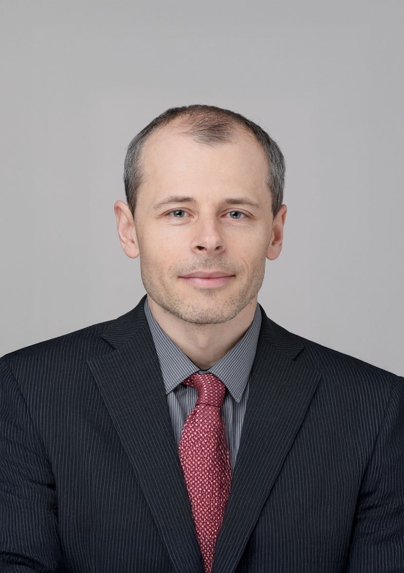
Czech Technical University in Prague(CTU), Czech Republic
Jiří Jakovenko
Professor Jiří Jakovenko is a distinguished academic and researcher in the field of IC design and microelectronics. He currently serves as Vice-Dean for Master's Studies at the Faculty of Electrical Engineering, Czech Technical University in Prague (CTU FEL), where he also holds a professorship at the Department of Microelectronics. His academic journey includes earning the titles of Full Professor (2022), Associate Professor (2013), and PhD (2004) from CTU FEL, with specialisations in electronics, MEMS structures, and sensor technologies.
As a professor, he leads research projects, supervises PhD and master's students, and teaches courses in subjects such as integrated circuit design and microelectronics. He also heads the laboratory for IC and MEMS design. His earlier roles included serving as an external consultant for Cadence Design Systems in San Jose, USA (2005–2008), where he contributed to RFIC design and Verilog AMS modelling for WLAN transceivers.
Professor Jakovenko's research spans analog and mixed-signal IC design, LED lighting technologies, and MEMS-based microsystems. He has participated in numerous international and national projects, includingH2020 initiatives, ENIAC, NATO Science for Peace, and Czech national grants. Notable projects include ACDRC (2024), Czech Competence Semiconductor Centre(2024), and Analog/Mixed-Signal Design Automation using AI (2020–2024).
In teaching, he covers bachelor's, master's, and doctoral courses in microelectronics, IC design, VLSI technologies, and System-on-Chip. He has supervised over ten PhD students and led international student mobility programs, including double-degree partnerships with RWTH Aachen and National TUST.
TOPIC: AI and Optimization for Electronic Design Automation(EDA)
Europe faces a significant challenge in reducing its dependence on imports of chips and semiconductor components from the rest of the world. The development of the semiconductor industry in Europe is based on the so-called EU Chips Act. The Czech Republic is a significant part of this chain with its own plan conceived in the National Semiconductor Strategy, recently approved by the Czech government. The strategy aims to establish astable domestic research, development, and production base in the field of semiconductors and semiconductor technologies.
An important part of this development is also cooperation with Taiwanese institutions, in which the ACDRC (Advanced Chip Design Research Centre) project plays a major role. The project is coordinated by the National Applied Science Laboratories NIAR Labs in Taiwan and three leading universities in the Czech Republic that cooperate in the field of semiconductors: the Czech Technical University in Prague, the Technical University in Brno, and Masaryk University. The ACDRC centre aims to contribute to the technological development of the semiconductor industry and enhance human resource capacity.
In the field of education, the cooperation between the Czech and Taiwanese parties focuses on coordinating and supporting education in the field of chip design and semiconductor technologies to prepare new experts, especially in advanced forms of education of master's and doctoral studies at Czech universities. The centre will also offer a scholarship program, organise advanced courses in cooperation with universities in the Czech Republic and Taiwan and conduct summer and winter schools. In the field of research, the primary goal of the ACDRC is to foster collaboration between the Czech Republic and Taiwan companies, enabling the effective exchange of knowledge and experience to support cooperation between academia and industry. The ACDRC coordinates the implementation of several research projects, including the development of an AI processor for the automotive industry and hardware security technology. Supported research areas also include chip cybersecurity, a backend tool for electrical automation of integrated circuit design, artificial intelligence on chips, bio-chips, and equipment for quality control and testing of SiCtechnology. The research and educational activities will primarily take place at the participating universities in Prague and Brno, where specialised laboratories will be expanded simultaneously.
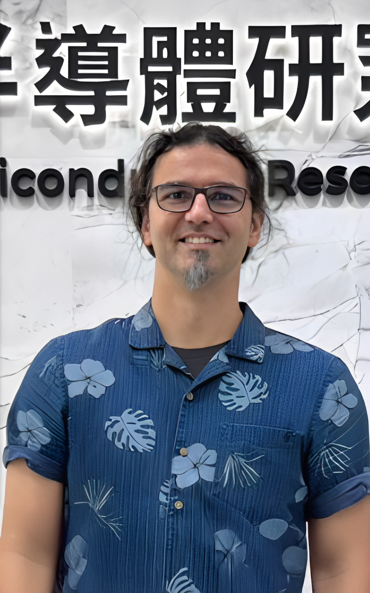
STMicroelectronics
Dalibor Barri
Ing. Dalibor Barri, Ph.D., is a highly specialized expert operating at the critical intersection of academic microelectronics research and high-volume industrial semiconductor design. His research focused on the Improvements in the Electrical Performances of MOSFETs in Integrated Circuits by Physical Mask Design, including investigations into advanced device structures like Trench MOS with waffle patterns. Concurrently, Dr. Barri has built a robust industrial career, currently serving as an R&D Layout Manager and Key Project Layout Leader at STMicroelectronics (since 2015,following an earlier tenure from 2007-2010). His core expertise lies in the advanced physical design and verification of Analog and Mixed-Signal (AMS)Integrated Circuits. He is a recognized solver and consultant for complex layout issues (e.g., Latch-up, Snap-Back, WPE, STI, LOD), and possesses deep technological experience across numerous process nodes, including BCD10, HCMOS, and TSMC (down to 55nm/C028FDSOI). Dr. Barri is a leader in automating physical design methodologies, defining top-down/bottom-up approaches for full symmetry layout, and developing extensive custom SKILL, Python, and Perl scripts for both layout efficiency and design optimization (e.g., gm/id methodology calculators). His background highlights a unique combination of device-level optimization (academic focus) and manufacturability-driven physical implementation (industry focus), making him a vital bridge between theoretical performance enhancement and production-ready IC design.
TOPIC: AI and Optimization for Electronic Design Automation(EDA)
Europe faces a significant challenge in reducing its dependence on imports of chips and semiconductor components from the rest of the world. The development of the semiconductor industry in Europe is based on the so-called EU Chips Act. The Czech Republic is a significant part of this chain with its own plan conceived in the National Semiconductor Strategy, recently approved by the Czech government. The strategy aims to establish astable domestic research, development, and production base in the field of semiconductors and semiconductor technologies.
An important part of this development is also cooperation with Taiwanese institutions, in which the ACDRC (Advanced Chip Design Research Centre) project plays a major role. The project is coordinated by the National Applied Science Laboratories NIAR Labs in Taiwan and three leading universities in the Czech Republic that cooperate in the field of semiconductors: the Czech Technical University in Prague, the Technical University in Brno, and Masaryk University. The ACDRC centre aims to contribute to the technological development of the semiconductor industry and enhance human resource capacity.
In the field of education, the cooperation between the Czech and Taiwanese parties focuses on coordinating and supporting education in the field of chip design and semiconductor technologies to prepare new experts, especially in advanced forms of education of master's and doctoral studies at Czech universities. The centre will also offer a scholarship program, organise advanced courses in cooperation with universities in the Czech Republic and Taiwan and conduct summer and winter schools. In the field of research, the primary goal of the ACDRC is to foster collaboration between the Czech Republic and Taiwan companies, enabling the effective exchange of knowledge and experience to support cooperation between academia and industry. The ACDRC coordinates the implementation of several research projects, including the development of an AI processor for the automotive industry and hardware security technology. Supported research areas also include chip cybersecurity, a backend tool for electrical automation of integrated circuit design, artificial intelligence on chips, bio-chips, and equipment for quality control and testing of SiCtechnology. The research and educational activities will primarily take place at the participating universities in Prague and Brno, where specialised laboratories will be expanded simultaneously.
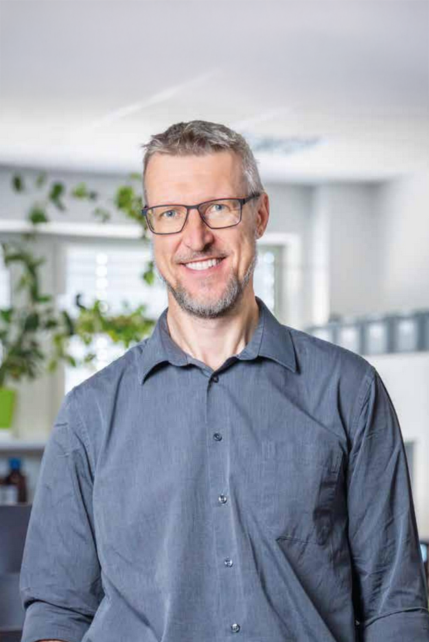
Brno University of Technology(BUT), Germany
Jiří Haze
Work Experience
2014–present — Head of Department of Microelectronics, Brno University of Technology (FEEC)
2010–2022 — Vice-Dean for External Relations, FEEC BUT
2009–present — Associate Professor, FEEC BUT (specialization in design, modelling, and fabrication of analog and mixed‑signal integrated circuits, sensor applications)
2005–2009 — Assistant Professor, FEEC BUT (specialization in design, modelling, and fabrication of analog and mixed‑signal integrated circuits, sensor applications)
International Experience
2024 — Invited lecture on chip design and semiconductor technologies, National Chung Hsing University, Taiwan
2008 — Lecturer and instructor, Rovira i Virgili University, Tarragona, Spain
2003 — Industry internship – design and development of integrated circuits, Institut für Mikroelektronik und Mechatronik‑Systeme, Germany
Memberships
Czech National Semiconductor Cluster
Silicon Europe
Executive University Coordinator — BUT Semiconductor Technology Hub
ELC IMAPS Europe
Member of scientific and study boards and associations
Reviewer for national and international projects, journals, and conferences
Additional Information
ORCID: https://orcid.org/0000-0001-5670-4283
H‑index: 4 (Web of Science), 5 (Scopus)
Publications: 37 (WoS), 46 (Scopus)
Citations: 53 (WoS), 84 (Scopus)
Selected Publications
• Kledrowetz, V., Prokop, R., Fujcik, L., Háze, J. Asynchronous delta‑sigma modulator in 28 nm FDSOI technology. Engineering Science and Technology, 2024.
• Kledrowetz, V., Prokop, R., Fujcik, L., Háze, J. A Fully Differential Analog Front‑End for Signal Processing from EMG Sensor in 28 nm FDSOI Technology. Sensors, 2023.
• Myška, V., Levek, V., Burget, R., Kolařík, M., Šteffan, P., Háze, J. IoT mechatronic access control system ePRO 1.4. IEEE Consumer Electronics Magazine, 2023.
• Kledrowetz, V., Fujcik, L., Prokop, R., Háze, J. An Active Resistor With a Lower Sensitivity to Process Variations, and Its Application in Current Reference. IEEE Access, 2020.
• Kledrowetz, V., Fujcik, L., Prokop, R., Háze, J. A 1 V 92 dB SNDR 10 kHz Bandwidth Second‑Order Asynchronous Delta‑Sigma Modulator for Biomedical Signal Processing. Sensors, 2020.
Projects
• 2024–2028 — Creating Higher Education – Industry Programmes for the Semiconductor Industry of Europe (CHIPS of Europe), €9.53M — consortium member
• 2024–2027 — Advanced Chip Design Research Center, Taiwan, $9.50M — consortium member
• 2014–2015 — Nanopotentiostat for medicine, €100k — project leader
• 2006–2011 — Research of new MEMS mechatronic structures, €2.85M — project coordinator
• 2011–2013 — Novel Intelligent Submicron Structures and Microsystems for Advanced Microsensors, €200k — research team member
Industrial Outputs
• Pekárek, J., Pavlík, M., Vlach, R., Vrba, R., Magát, M., Háze, J., Mareček, K. Device for anodic bonding — Utility model, 2011.
• Háze, J., Bohrn, M., Fujcik, L., Kledrowetz, V., Pavlík, M., Prokop, R. Potentiostat — Patent, 2015.
TOPIC: Hardware Security Chip Design and Development
The presentation is focused on the design and development of particular stages of the novel security chip designed in collaboration with Jmem Technology Co., Ltd. in the framework of the ACDRC project. The BUT project team consists of professors and PhD students skilled in chip design.
First presented section deals with a design of a one-time-programmable (OTP) based physical unclonable function (PUF) array for secure key generation in hardware security applications. By leveraging intrinsic device-level process variations within PUF cells, the proposed architecture achieves high uniqueness and stability without requiring additional randomization circuitry. The design enables efficient, tamper-resistant key generation suitable for cryptographic modules and embedded security systems.
Second stage presents a design and hardware implementation of the Advanced Encryption Standard (AES)supporting AES-128, AES-192, and AES-256 variants, developed in a 22 nm technology. The design integrates an advanced masking scheme comprising eight distinct masking options to enhance resistance against side-channel attacks(SCA). Extensive architectural optimization enables high-speed operation exceeding 350 MHz, achieving superior encryption and decryption throughput while maintaining robust hardware-level security.
Last part depicts a design and implementation of phase-locked loop with full digital control (ADPLL)developed in 22 nm technology. The proposed design is optimized for minimal silicon area and enhanced robustness against disruptions from power supply, achieving stable operation across a high-speed frequency range from 512 MHz to1.016 GHz. A novel control circuitry is introduced to enable rapid phase-lock acquisition while providing effective protection against glitch attacks on the input reference clock.
The complete chip die is now under preparation for frabrication procedure. Next year the test and evaluation processes will be conducted to finalize the complete chip version design.
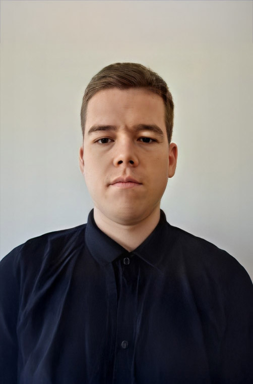
Czech Technical University(CTU), Czech
Jiří Maier
Jiří Maier was born in 1999 in the Czech Republic. He received master’s degree in 2024 from Czech Technical University and National Taiwan University of Science and Technology following a double-degree study of electronics and computer science. He is presently a Ph.D. student at Czech Technical University in Prague. His research interests are magnetic sensors and IC design. He also has experience with software engineering and embedded systems.
TOPIC: Micro-fluxgate with Racetrack Core and Solenoid Coils
In previous years, our team developed a CMOS-based micro-fluxgate [1] using a racetrack-shaped magnetic core and wire-bonded coils. Wire bonding provided better performance than flat coils. The amorphous metal core, laser-cut and optimized by reducing thickness from 25 μm to 10 μm,improved sensitivity, reduced noise, and lowered power consumption by decreasing eddy currents [2]. Annealing further enhanced magnetic properties, achieving noise below 1 nT/√Hz at 1 Hz, compared to 5 nT for TI’s DRV425,with sensitivity over 8000 V/T and power use of 100 mW, significantly less than the original 400 mW.
The CMOS chip allows easy integration of driving and processing electronics. We are developing pulse excitation and advanced signal processing using higher harmonics to boost sensitivity, along with feedback for closed-loop operation.
Since wire bonding is not suitable for mass production, the second-generation device will use flip-chip technology. It will consist of two bonded chips with the core in-between, with coils formed by metal layers and connections via gold bumps.